Vaishnaw Unveils Semicon 2.0 With ₹1.27 Lakh Cr Outlay
Synopsis
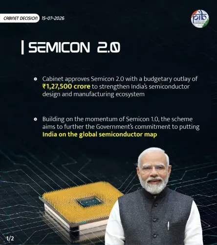
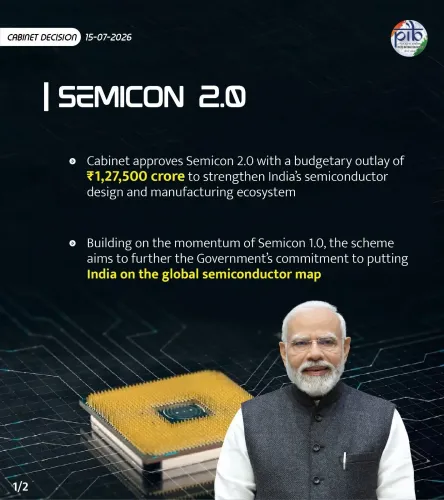
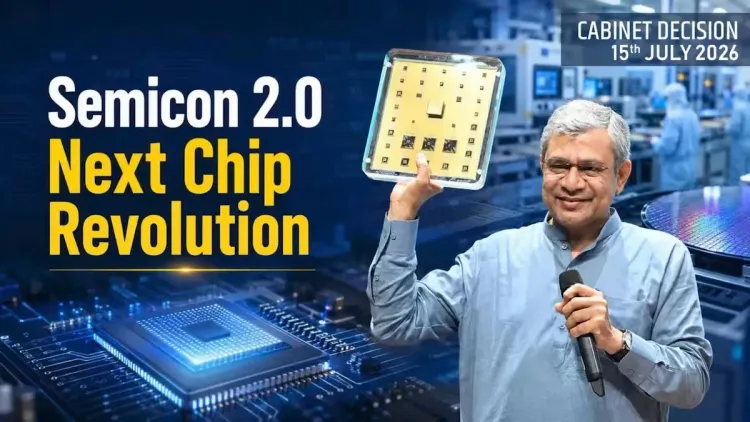
Union Minister Ashwini Vaishnaw announced Semicon 2.0 on 16 July 2026 with a ₹1,27,500 crore outlay targeting chip design, fabrication, ATMP/OSAT, R&D, machines and materials, and talent development — a major escalation of India's semiconductor ambitions.
Key Takeaways
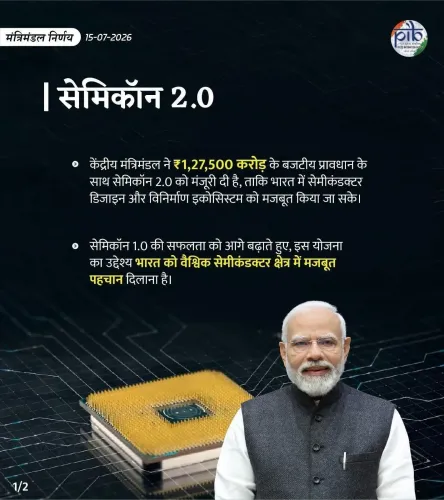
Semicon 2.0 carries a total outlay of ₹1,27,500 crore , announced by Union Minister Ashwini Vaishnaw on 16 July 2026 .
The policy is structured around six pillars : chip design, machines and materials, more fabs, ATMP/OSAT, R&D, and talent development.
It builds on the original India Semiconductor Mission approved in December 2021 with an outlay of approximately ₹76,000 crore .
The new package represents a significant funding increase and broadens the scope to cover the full semiconductor value chain.
A dedicated talent development pillar acknowledges workforce capacity as a critical constraint for India's chip ambitions.
Next steps include disbursement frameworks, new fab announcements, and potential global technology partnerships under MeitY .
Union Minister Ashwini Vaishnaw on Thursday, 16 July 2026 announced Semicon 2.0, a revamped semiconductor policy package with a total outlay of ₹1,27,500 crore, structured around six strategic pillars aimed at building a self-reliant chip ecosystem in India.
Context
In his post on X, Vaishnaw outlined the six pillars of Semicon 2.0: chip design, machines and materials, more fabrication units (fabs), strengthening ATMP/OSAT (assembly, testing, marking, and packaging / outsourced semiconductor assembly and test), research and development, and talent development. The announcement signals a significant scaling-up of India's ambitions in the global semiconductor value chain.
The six-pillar structure reflects a deliberate effort to address the full spectrum of semiconductor manufacturing — from the earliest design stage to the final packaging and testing of chips, as well as the human capital needed to sustain the industry long-term.
Policy Backdrop
Semicon 2.0 builds on the original India Semiconductor Mission (ISM), approved in December 2021 under the Ministry of Electronics and Information Technology (MeitY) with an initial outlay of approximately ₹76,000 crore. That programme sought to attract wafer fabrication plants and design-linked investments through fiscal incentives, making India a viable alternative to established East Asian chip-manufacturing hubs.
The new package, at ₹1,27,500 crore, represents a substantial increase over the original commitment, reflecting lessons learned from the first phase and the heightened global race to secure domestic semiconductor supply chains. India's approach draws broad parallels with the US CHIPS and Science Act and the EU Chips Act, while remaining anchored in the government's Atmanirbhar Bharat framework. The Production Linked Incentive (PLI) scheme for electronics, launched in 2020, laid earlier groundwork by incentivising mobile phone and component manufacturing.
Stakeholders and Impact
The policy is expected to have direct implications for domestic and global semiconductor firms, electronics manufacturers, and engineering graduates seeking careers in chip design and fabrication. The explicit inclusion of talent development as a dedicated pillar signals that the government recognises workforce capacity as a binding constraint alongside capital and technology.
The ATMP/OSAT pillar is particularly significant: assembly, testing, and packaging operations are often the entry point for countries building semiconductor capabilities, and strengthening this segment can attract global chip companies looking to diversify their supply chains away from concentrated East Asian production bases. A dedicated pillar for machines and materials also suggests intent to reduce dependence on imported semiconductor equipment and specialty chemicals.
What's Next
Attention will now turn to the disbursement timelines, eligibility criteria, and incentive structures that will govern the ₹1,27,500 crore outlay across the six pillars. Announcements of specific fab projects, design centre investments, and international technology partnerships are likely to follow as the policy framework is operationalised through MeitY.
If executed at scale, Semicon 2.0 could position India as a meaningful node in the global semiconductor supply chain by the end of this decade — a strategic outcome that carries both economic and national-security implications for the country's technology sovereignty.
Point of View
000 crore to ₹1,27,500 crore signals that the government is no longer treating semiconductors as a long-horizon aspiration but as an immediate industrial priority. The six-pillar architecture — spanning design, equipment, fabrication, packaging, R&D, and skilling — is notably more comprehensive than the first phase, suggesting the policy has absorbed the lesson that fab investment alone cannot build a sustainable ecosystem. Placing Vaishnaw, who also steers the Railways and I&B portfolios, as the face of this announcement underlines how central the electronics and technology brief has become within the BJP government's economic narrative. Whether the outlay translates into operational fabs and design centres will depend heavily on execution speed and the ability to attract credible global technology partners.
NationPress
16 Jul 2026
Frequently Asked Questions
What is Semicon 2.0 India?
Semicon 2.0 is India's upgraded semiconductor policy package announced by Union Minister Ashwini Vaishnaw on 16 July 2026, with a total outlay of ₹1,27,500 crore. It is designed to build domestic capabilities across six pillars: chip design, machines and materials, fabrication units, ATMP/OSAT, research and development, and talent development.
What is the total budget of Semicon 2.0?
The total outlay for Semicon 2.0 is ₹1,27,500 crore, as announced by Union Minister Ashwini Vaishnaw. This is a significant increase over the approximately ₹76,000 crore committed under the original India Semiconductor Mission approved in December 2021.
What are the six pillars of Semicon 2.0?
The six pillars of Semicon 2.0 are: (1) chip design, (2) machines and materials, (3) more fabrication units (fabs), (4) strengthening ATMP/OSAT (assembly, testing, marking, packaging and outsourced semiconductor assembly and test), (5) research and development, and (6) talent development.
What is ATMP/OSAT in the context of India's semiconductor policy?
ATMP stands for assembly, testing, marking, and packaging, while OSAT refers to outsourced semiconductor assembly and test. These are the final stages of chip manufacturing and are often an entry point for countries building semiconductor capabilities. Semicon 2.0 dedicates a specific pillar to strengthening this segment in India.
How does Semicon 2.0 differ from the original India Semiconductor Mission?
The original India Semiconductor Mission, approved in December 2021, had an outlay of approximately ₹76,000 crore and focused primarily on attracting fabrication plants and design-linked investments. Semicon 2.0 raises the outlay to ₹1,27,500 crore and takes a broader six-pillar approach that explicitly includes machines and materials, R&D, and talent development alongside fabs and chip design.