Will the Centre Invest Rs 4,500 Crore to Upgrade the Semiconductor Laboratory in Mohali?

Synopsis
In a landmark decision, the Centre plans to invest Rs 4,500 crore to modernize the Semiconductor Laboratory in Mohali, ensuring it remains a government entity. This significant upgrade aims to enhance India's chip production capabilities, supporting innovation and entrepreneurship across the nation.
Key Takeaways
The Centre is investing Rs 4,500 crore to upgrade SCL Mohali.
SCL will remain a government entity and will not be privatized.
The investment aims to increase chip production capacity by 100 times.
Students and startups will benefit from enhanced fabrication facilities.
The initiative supports India's vision for self-reliance in technology.
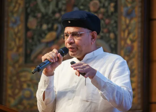
Mohali (Punjab), Nov 28 (NationPress) - On Friday, Union Electronics and Information Technology Minister Ashwini Vaishnaw declared that the Central Government is set to invest Rs 4,500 crore for the enhancement and expansion of the Semiconductor Laboratory (SCL) in Mohali.
During his tour in Mohali, the minister stated: "Undoubtedly, SCL Mohali will undergo a significant modernization, and it will remain under government control. A remarkable journey lies ahead, and India is poised for it."
Vaishnaw mentioned that Prime Minister Narendra Modi has laid out a definitive roadmap for SCL Mohali. The primary vision includes modernizing the facility with a government-backed investment of Rs 4,500 crore, which aims to drastically enhance production, targeting a 100-fold increase in wafer output from the current levels.
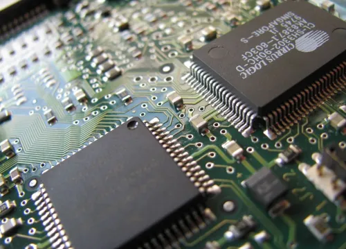
SCL Mohali will persist in its support for students, researchers, and startups by offering fabrication facilities that can translate their chip designs into actual silicon.
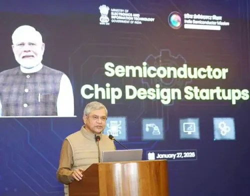
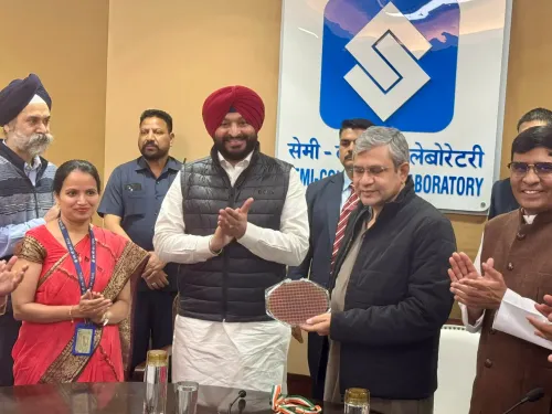
The laboratory will continue to serve as a hub for talent cultivation, innovation, and startup growth. The fabrication assistance provided by SCL thus far will see further expansion in the future. To facilitate the ongoing modernization plan of SCL, the Centre has requested the Punjab government to allocate 25 acres of land, as stated by Vaishnaw during a program where 28 chips designed by students from 17 academic institutions were presented.
These chips were designed using Electronic Design Automation (EDA) tools made available to students through the Chips to Start-up (C2S) initiative. Overall, 56 chips designed by students have been successfully fabricated at SCL as part of this initiative.
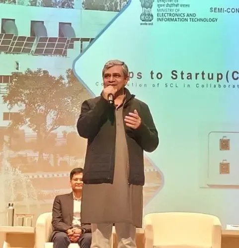
The minister also inaugurated the Semiconductor Process Gallery and the Abhyuthanam Training Block. The Semiconductor Process Gallery features a cleanroom lab stocked with earlier-generation fabrication tools, providing students with a practical experience of a semiconductor fabrication and ATMP facility. The Abhyuthanam Training Block offers both online and offline semiconductor training modules, along with hands-on fire and safety training.
Vaishnaw emphasized that India stands out as one of the few nations where students from nearly 300 universities are designing semiconductor chips using top-tier EDA tools provided through government initiatives. This ecosystem is truly one of a kind globally, he remarked.
The minister concluded by stating that self-sufficiency in critical sectors is vital, and India aims to establish a robust ecosystem for indigenous chip development.
A strong consortium comprising the CDAC, DRDO, and other organizations will collaborate on the design, product development, and manufacturing of homegrown chips.
Point of View
I believe this investment in the Semiconductor Laboratory is a crucial step towards enhancing India's technological capabilities and self-reliance in a strategic sector. It showcases the government's commitment to fostering innovation and supporting the next generation of engineers, researchers, and entrepreneurs.
NationPress
2 Jul 2026
Frequently Asked Questions
What is the purpose of the Rs 4,500 crore investment?
The investment aims to upgrade and expand the Semiconductor Laboratory (SCL) in Mohali, enhancing production capacity and supporting research and startups.
Who announced the investment?
Union Electronics and Information Technology Minister Ashwini Vaishnaw announced the investment during his visit to Mohali.
How will the investment affect students and researchers?
The upgraded facility will provide better fabrication support for students and researchers, helping them turn their chip designs into actual silicon.
What is the Chips to Start-up (C2S) program?
The C2S program provides students with access to Electronic Design Automation (EDA) tools to design semiconductor chips.
What is the significance of self-reliance in chip development?
Self-reliance in chip development is vital for national security and economic independence, reducing reliance on foreign technology.