Delhi-NCR Educational Institutions Propel India Semiconductor Mission: Minister
Synopsis
Union Minister Ashwini Vaishnaw highlights the crucial role played by major educational institutions in the Delhi-NCR region in advancing the India Semiconductor Mission, paving the way for a skilled workforce in semiconductor design and innovation.
Key Takeaways
Educational institutions in Delhi-NCR are key players in the India Semiconductor Mission .
Students receive training in semiconductor design and manufacturing.
World-class EDA tools are provided for hands-on experience.
The initiative is expanding to 500 universities to enhance the talent pool.
Projected demand for 2 million skilled professionals in the semiconductor sector.
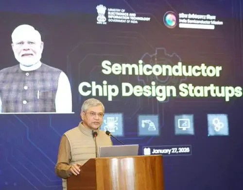
New Delhi, March 7 (NationPress) Union Minister Ashwini Vaishnaw announced on Saturday that numerous prominent educational institutions within the Delhi-National Capital Region (NCR) are significantly contributing to the India Semiconductor Mission (ISM). These institutions are instrumental in providing education and training in semiconductor design, testing, and validation.
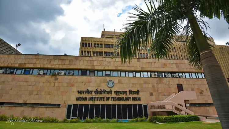
Notable institutions include Indian Institute of Technology, Delhi; National Institute of Technology Delhi; Indraprastha Institute of Information Technology Delhi; Delhi Technological University; Netaji Subhas University of Technology; Jawaharlal Nehru University; Indira Gandhi Delhi Technical University for Women; Vivekananda Institute of Professional Studies; and DV2JS Innovation LLP, all located in New Delhi.
Utilizing cutting-edge Electronic Design Automation (EDA) tools, students in these institutions are actively engaged in the design of actual semiconductor chips, thereby supporting India in cultivating a robust talent pool for its semiconductor industry, as stated by the minister.
The Indian government, through the Semicon 2.0 initiative, is dedicated to fostering semiconductor design, manufacturing, and innovation nationwide, aiming to position India as a leading global hub for semiconductor talent and manufacturing.
Vaishnaw also shared that world-class EDA tools backed by Synopsys, Cadence, Siemens, Renesas, Ansys, and AMD have been integrated into 315 academic institutions throughout the country.
These tools grant students hands-on experience in semiconductor chip design, with real chips being fabricated and tested at the Semiconductor Laboratory (SCL) in Mohali, providing comprehensive exposure from design to fabrication, packaging, and testing.
This initiative has emerged as the world’s largest open-access EDA program, boasting over 1.85 crore hours of EDA tool utilization for chip design training, with continuous growth.
The minister emphasized that students from universities nationwide, spanning from Assam to Gujarat and Kashmir to Kanyakumari, are actively engaged in semiconductor design. Under the Semicon 2.0 framework, this program is set to expand from 315 to 500 universities, thereby establishing a formidable base of skilled engineers across the country.
As the global semiconductor market approaches a valuation of $2 trillion, nearly 2 million skilled professionals will be required, thereby creating unprecedented job opportunities for the youth of India.
Point of View
The engagement of educational institutions in the India Semiconductor Mission is a vital step towards enhancing India's position in the global semiconductor market. The collaboration between academia and industry signifies a forward-looking approach to skill development, essential for the nation's technological advancements.
NationPress
5 Jul 2026
Frequently Asked Questions
What is the India Semiconductor Mission?
The India Semiconductor Mission aims to promote semiconductor design, manufacturing, and innovation in the country, establishing India as a global hub for semiconductor talent.
Which institutions are involved in this initiative?
Key institutions include IIT Delhi, National Institute of Technology Delhi, Indraprastha Institute of Information Technology, and several others across the NCR.
How are students benefiting from this program?
Students gain practical experience by designing real semiconductor chips using advanced EDA tools, preparing them for careers in the semiconductor industry.
What is the goal of expanding the program to 500 universities?
The expansion aims to create a robust talent pool of skilled engineers across India, enhancing the workforce needed for the growing semiconductor industry.
Why is the semiconductor industry important?
The semiconductor industry is crucial as it is projected to reach a global value of $2 trillion, creating significant job opportunities for skilled professionals.