India's Ambitious Plan: Training 85,000 Semiconductor Engineers Under C2S Initiative

Synopsis
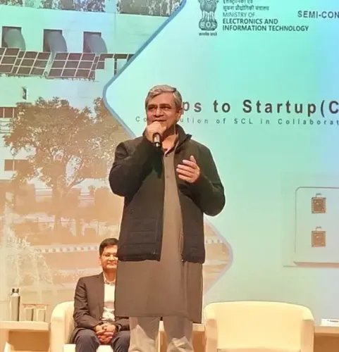
India is on track to train 85,000 semiconductor design engineers as part of its Chips to Startups initiative, according to Union Minister Ashwini Vaishnaw, who highlighted the program's significance for the country's tech ecosystem.
Key Takeaways
India is training 85,000 semiconductor engineers.
The initiative is part of the Chips to Startups (C2S) program.
EDA tools from global firms are now available in 315 institutions.
Hands-on training is provided through the Semiconductor Laboratory in Mohali.
The semiconductor market is expected to grow to nearly $2 trillion.
New Delhi, March 7 (NationPress) India is making significant strides towards its goal of training 85,000 semiconductor design engineers as part of the Chips to Startups (C2S) initiative, announced Union Minister Ashwini Vaishnaw on Saturday.
The minister emphasized the government's commitment to enhancing talent development within the semiconductor industry.
This program is a critical component of the India Semiconductor Mission (ISM), which concentrates on training, upskilling, and workforce development to establish a solid talent pipeline for the nation's burgeoning chip ecosystem. Vaishnaw noted that substantial progress has been achieved within the first four years of the decade-long C2S initiative.
“Top-tier Electronic Design Automation (EDA) tools from leading global tech firms like Synopsys, Cadence Design Systems, Siemens, Renesas Electronics, Ansys, and AMD are now accessible at 315 educational institutions across India,” he stated.
These tools enable students to acquire practical skills in semiconductor chip design.
The chips crafted by students are being produced and evaluated at the Semiconductor Laboratory (SCL) in Mohali, allowing them to gain hands-on experience throughout the entire process—from design to fabrication, packaging, and testing.
He also highlighted that the initiative has evolved into the largest open-access EDA program globally, with over 1.85 crore hours of EDA tool usage logged for chip design training.
Students from universities nationwide, spanning from Assam to Gujarat and Jammu and Kashmir to Tamil Nadu, are now actively engaged in semiconductor design activities, he added.
Pointing to global industry trends, Vaishnaw remarked that the semiconductor industry is projected to expand from its current valuation of $800–900 billion to nearly $2 trillion, resulting in a demand for approximately two million skilled professionals worldwide and creating substantial employment opportunities for the youth of India.
He also revealed that under the ‘India Semiconductor Mission 2.0,’ the initiative will extend from 315 to 500 academic institutions, thereby enhancing the talent pipeline in semiconductor design, fabrication, packaging, and testing across all regions.
Point of View
The ambitious goal of training 85,000 engineers reflects a strategic move to harness India's vast talent pool. This initiative not only promises to meet the growing demands of the semiconductor market but also opens up significant employment opportunities for the youth, positioning India favorably in the global tech landscape.
NationPress
29 Jun 2026
Frequently Asked Questions
What is the Chips to Startups initiative?
The Chips to Startups initiative is a program aimed at training and upskilling engineers in semiconductor design to develop a robust talent pipeline in India's semiconductor industry.
How many engineers will be trained under this initiative?
The initiative aims to train 85,000 semiconductor design engineers over a period of ten years.
What are EDA tools, and why are they important?
Electronic Design Automation (EDA) tools are software applications used for designing and testing semiconductor chips, providing students with practical experience in chip design.
How will this initiative impact job opportunities in India?
With the semiconductor industry projected to grow significantly, the initiative is expected to create substantial job opportunities for skilled professionals in India.
What is the India Semiconductor Mission 2.0?
The India Semiconductor Mission 2.0 is an expansion of the current initiative, increasing the number of academic institutions involved from 315 to 500 to strengthen the semiconductor talent pipeline.