India's DLI scheme bears fruit: Netrasemi's Edge AI chip 'NETRA A2000' clears silicon bringup
Synopsis
India's DLI scheme has produced its most tangible result yet: a domestically designed Edge AI chip — Netrasemi's NETRA A2000 — has cleared silicon bringup at TSMC's 12nm node and is headed for commercial production. It is the first flagship AI SoC to emerge from MeitY's incentive pipeline, and a proof point that India can design globally competitive chip IP.
Key Takeaways
Netrasemi , a Thiruvananthapuram -based fabless startup, has completed silicon bringup of India's first Edge AI SoC, the NETRA A2000 , at the 12nm technology node .
The chip targets surveillance, automotive, robotics, and drones , with real-time video analytics and on-device AI capabilities.
Netrasemi was among the first four startups to receive ₹15 crore DLI support from MeitY in 2023 ; total funding raised stands at ₹125 crore .
Commercial production at TSMC, Taiwan is expected to begin next year, with chip designs being shared with select OEMs for joint R&D.
Union Minister Ashwini Vaishnaw cited the milestone as evidence that India's Design-Linked Incentive (DLI) and Design Infrastructure Support (DIS) schemes are working.
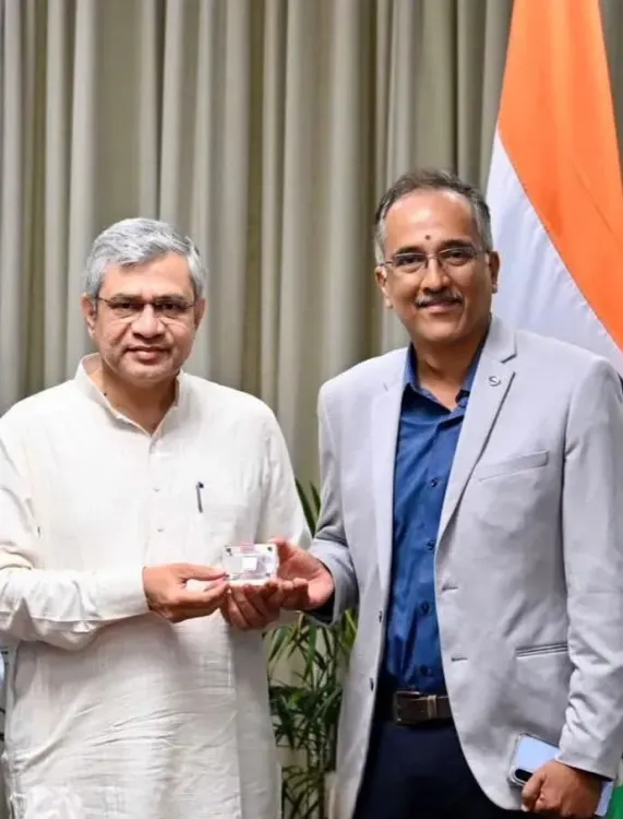
India's design-linked incentive (DLI) scheme is delivering tangible results, with Union Minister Ashwini Vaishnaw highlighting the successful silicon bringup of the country's first flagship Edge AI System-on-Chip (SoC), the 'NETRA A2000', designed at the advanced 12nm technology node by Thiruvananthapuram-based fabless semiconductor startup Netrasemi. The chip is now being readied for commercial production, marking a significant milestone for India's domestic semiconductor ambitions.
What the NETRA A2000 Chip Does
The NETRA A2000 is built for high-performance, real-time Edge AI applications — powering smart vision devices across surveillance, automotive, robotics, and drones. It integrates smart vision capabilities and real-time video analytics, enabling on-device AI for smart cameras and Edge AI platforms without reliance on cloud processing.
The chip is fabricated at TSMC's 12nm advanced process node in Taiwan and targets high-TOPS AI performance, computer vision, video streaming, secure boot, and significant I/O capabilities. It features Netrasemi's in-house Neural Processor (NPU), Vision Cores (VPU), Image Signal Processor (ISP), Crypto-Engines, and other hardware acceleration IP cores, alongside the company's patented Heterogeneous Graph-Stream Parallel Processing architecture.
What the Government Said
Minister Vaishnaw took to X to applaud the achievement, posting: 'Netrasemi has designed India's first Edge AI System-on-Chip (SoC) 'NETRA A2000', at advanced 12 nm node. At commercial scale, this will power smart vision devices for surveillance, automotive, robotics, drones, etc.'
The minister framed the development as direct evidence of the DLI scheme's effectiveness, noting that both the Design-Linked Incentive (DLI) and Design Infrastructure Support (DIS) schemes played a key role in reaching this milestone.
Role of the DLI Scheme
Netrasemi was among the first four startups selected for ₹15 crore DLI support in 2023 by the Ministry of Electronics and Information Technology (MeitY). The company has since raised a total of ₹125 crore in funding. The DLI scheme, part of India's broader semiconductor push, provides financial incentives and infrastructure access to domestic chip design firms — an ecosystem that did not meaningfully exist in India a decade ago.
Commercial Roadmap and Industry Partnerships
'Our SoCs go beyond conventional AI/ML integration by combining proprietary hardware acceleration IPs with domain-specific optimisations tailored for high-performance, real-time edge AI,' said Jyothis Indirabhai, Co-founder and CEO of Netrasemi.
'We are currently working with several leading OEMs to facilitate early sample evaluations, co-development, and advanced R&D initiatives,' Indirabhai added. The chip design is being shared with select Original Equipment Manufacturers (OEMs) for joint R&D to develop further commercial use cases. According to the startup, commercial production at TSMC, Taiwan is likely to begin next year.
What This Means for India's Semiconductor Ambitions
This comes amid India's accelerating push to build a domestic semiconductor ecosystem, backed by the government's ₹76,000 crore India Semiconductor Mission. The NETRA A2000 represents the first concrete design-to-silicon outcome from the DLI pipeline — a proof point that India can produce globally competitive chip IP, even if fabrication currently remains offshore. The next test will be whether such designs can anchor domestic manufacturing partnerships as India's fab infrastructure matures.
Point of View
But it also exposes the limits of India's semiconductor ambition: the chip was designed in Thiruvananthapuram and fabricated in Taiwan. Until India has domestic fab capacity at advanced nodes, 'Made in India' chip design will remain a half-loop. The DLI scheme deserves credit for seeding a design ecosystem that barely existed — but the harder question is whether these startups can survive the commercialisation gap between a successful bringup and a profitable product. Netrasemi's OEM co-development path is the right instinct; execution at scale is where most fabless startups globally have stumbled.
NationPress
14 Oct 2026
Frequently Asked Questions
What is India's NETRA A2000 chip?
The NETRA A2000 is India's first flagship Edge AI System-on-Chip (SoC), designed by Thiruvananthapuram-based startup Netrasemi at TSMC's advanced 12nm process node. It is built for real-time AI applications including smart surveillance, automotive systems, robotics, and drones.
What is the Design-Linked Incentive (DLI) scheme?
The DLI scheme is a MeitY-backed programme that provides financial incentives and infrastructure support to Indian semiconductor design startups. Netrasemi received ₹15 crore under the scheme in 2023 as one of the first four selected startups.
When will the NETRA A2000 enter commercial production?
According to Netrasemi, commercial production at TSMC in Taiwan is expected to begin next year. The chip design is currently being shared with select OEMs for early sample evaluations and joint R&D.
What makes the NETRA A2000 technically significant?
The chip integrates an in-house Neural Processor (NPU), Vision Cores (VPU), Image Signal Processor (ISP), Crypto-Engines, and Netrasemi's patented Heterogeneous Graph-Stream Parallel Processing architecture — targeting high-TOPS AI performance without cloud dependency.
Who is behind Netrasemi and how much has it raised?
Netrasemi is a fabless semiconductor startup based in Thiruvananthapuram, co-founded by Jyothis Indirabhai, who serves as CEO. The company has raised a total of ₹125 crore in funding to date.