Vaishnaw Flags DLI Win as Netra Semi Designs India's First Edge AI SoC
Synopsis
Union Minister Ashwini Vaishnaw has flagged Netra Semi's NETRA A2000 — India's first Edge AI SoC at 12 nm — as a concrete outcome of the government's Design Linked Incentive scheme, underscoring India's push to build a domestic semiconductor design ecosystem.
Key Takeaways
Union Minister Ashwini Vaishnaw publicly cited the Design Linked Incentive (DLI) scheme as 'showing good results' on 29 May 2026 .
Netra Semi has designed the NETRA A2000 , described as India's first Edge AI System-on-Chip, at an advanced 12 nm node .
At commercial scale, the chip is targeted at smart vision applications including surveillance, automotive, robotics, and drones .
The DLI scheme was approved in December 2021 with an outlay of ₹1,519 crore over five years under the India Semiconductor Mission .
The milestone signals growing maturity in India's fabless semiconductor design sector, though the path to volume production remains the key next step.
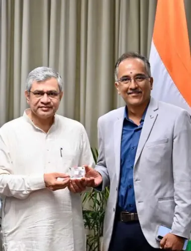
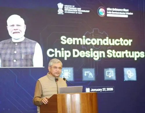
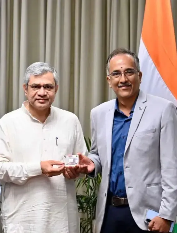
Union Minister Ashwini Vaishnaw on Friday, 29 May 2026 highlighted a milestone under the government's Design Linked Incentive (DLI) scheme, pointing to Netra Semi's development of India's first Edge AI System-on-Chip (SoC), the NETRA A2000, as evidence that the scheme is delivering results.
Context
The minister's post on X drew attention to Netra Semi, an Indian fabless semiconductor startup, which has designed the NETRA A2000 — described as India's first Edge AI SoC — at an advanced 12 nm node. According to the post, the chip is intended at commercial scale to power smart vision devices for applications spanning surveillance, automotive, robotics, and drones. The announcement marks a visible output from a scheme that has been operational for several years but has faced questions about tangible commercial results.
Policy Backdrop
The Design Linked Incentive (DLI) scheme was approved by the Union Cabinet in December 2021 with a total outlay of ₹1,519 crore over five years. It was designed to offer financial incentives to domestic semiconductor design companies focused on intellectual property development and product commercialisation. The scheme is administered under the India Semiconductor Mission (ISM), the nodal agency set up within the Ministry of Electronics and Information Technology (MeitY) to build a comprehensive domestic semiconductor ecosystem — covering design, packaging, and manufacturing.
The DLI scheme sits alongside larger production-linked incentive programmes for electronics manufacturing, forming part of India's multi-year strategy since 2021 to reduce dependence on imported chips and cultivate indigenous semiconductor capability. Vaishnaw, who holds the Electronics and IT portfolio in addition to Railways and Information and Broadcasting, has been the political face of this push.
Stakeholders and Impact
For Indian semiconductor startups and AI hardware firms, the NETRA A2000 represents a proof-of-concept that the DLI framework can support chips reaching commercially viable process nodes. Edge AI chips — designed to run artificial intelligence workloads locally on devices rather than in the cloud — are in growing demand globally across surveillance infrastructure, automotive safety systems, industrial robotics, and unmanned aerial vehicles. A domestically designed SoC at 12 nm would, if it reaches volume production, reduce India's reliance on foreign chip designers for these categories.
The beneficiaries extend beyond Netra Semi itself. A credible DLI success story strengthens the case for other startups to invest in chip design in India, and signals to global semiconductor supply-chain players that Indian design houses are maturing. Defence and automotive procurement programmes have been cited by policymakers as potential end-markets for domestically designed chips.
What's Next
The immediate question is whether the NETRA A2000 progresses from design completion to volume manufacturing and commercial deployment. Chip design at an advanced node is a significant achievement, but the path to mass production involves foundry partnerships, customer qualification, and sustained funding — steps that will determine whether this milestone translates into market impact. Observers will also watch MeitY's periodic progress disclosures for data on additional DLI-approved designs, and any announcements linking domestically designed chips to government procurement in defence or automotive sectors. Vaishnaw's public endorsement adds political weight to Netra Semi's profile, potentially accelerating conversations with both investors and institutional buyers.
Point of View
Which is the harder and more credible benchmark. The choice of Edge AI as the showcase application is also strategic: it maps directly onto high-growth sectors — defence surveillance, automotive, drones — where India has both policy priority and import-substitution motivation. If Netra Semi can convert this design win into production volumes, it becomes a template the government will replicate to justify and expand the DLI outlay.
NationPress
12 Oct 2026
Frequently Asked Questions
What is the Design Linked Incentive (DLI) scheme?
The DLI scheme is a government programme approved in December 2021 with an outlay of ₹1,519 crore over five years to provide financial incentives to Indian semiconductor design companies for developing intellectual property and commercialising chip products.
What is the NETRA A2000 chip?
The NETRA A2000 is described as India's first Edge AI System-on-Chip (SoC), designed by Netra Semi at a 12 nm process node, intended to power smart vision devices for surveillance, automotive, robotics, and drone applications.
What is an Edge AI SoC and why does it matter for India?
An Edge AI SoC is a chip that runs artificial intelligence workloads directly on a device rather than in the cloud, enabling real-time processing for cameras, vehicles, and robots. A domestically designed version reduces India's dependence on foreign chip suppliers for these fast-growing application areas.
Who oversees India's semiconductor policy?
The India Semiconductor Mission (ISM), under the Ministry of Electronics and Information Technology (MeitY), is the nodal agency. Union Minister Ashwini Vaishnaw holds the Electronics and IT portfolio and is the senior political figure overseeing semiconductor and electronics policy.