Dholera ITI graduates India's first semiconductor cleanroom batch, 16 trained
Synopsis
India's first ITI-integrated semiconductor cleanroom has produced its debut batch of 16 trained precision welders in Dholera — a privately funded, ISO Class 1-equivalent facility that costs the government nothing but feeds directly into Gujarat's ₹1.25 lakh crore chip manufacturing pipeline. With a second batch already underway, this is a rare instance of vocational training keeping pace with industrial ambition.
Key Takeaways
16 students have graduated from India's first ITI-based semiconductor cleanroom skilling programme at ITI Dholera , Gujarat.
The UHP Semiconductor Welding Programme runs for six weeks , with 70 per cent of the curriculum hands-on.
The cleanroom facility is a containerised ISO Class 1-equivalent environment, fully financed and operated by the private partner — no capital expenditure by the government.
Graduates are certified as UHP precision welders and their profiles are shared directly with contractors on semiconductor projects in Dholera .
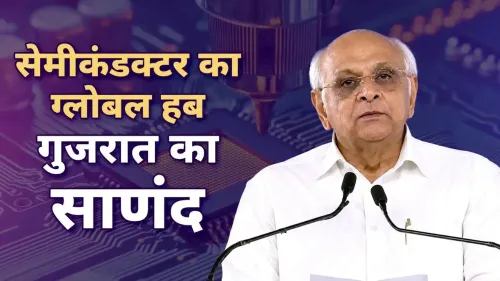
Gujarat accounts for nearly 40 per cent of India's approved semiconductor manufacturing capacity, with cumulative investments of approximately ₹1.25 lakh crore .
A second batch of trainees has already commenced training at the same facility.
India's first Industrial Training Institute (ITI)-based semiconductor cleanroom skilling programme has produced its inaugural batch of 16 graduates from the ITI Dholera facility in Gujarat, marking a concrete step toward building a domestic workforce for the country's fast-growing chip manufacturing sector.
About the Programme
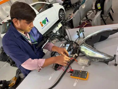
The UHP Semiconductor Welding Programme is a six-week course structured in two phases: two weeks of foundational instruction at a skills institute in Ahmedabad, followed by four weeks of advanced practical training at the ITI Dholera cleanroom facility. Approximately 70 per cent of the curriculum is hands-on, covering orbital welding, infrared fusion welding, helium leak testing, pressure testing, precision tube preparation, cleanroom behaviour protocols, and quality inspection practices.
The second batch of trainees has already commenced training at the same facility, signalling the programme's intent to run continuously rather than as a one-off pilot.
The Cleanroom Facility
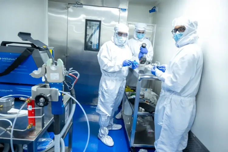
The cleanroom at ITI Dholera has been developed as a containerised ISO Class 1-equivalent environment, equipped with orbital welding machines, IR fusion welding units, leak detection systems, pressure testing setups, air locks, and air shower systems. Notably, the facility has been fully financed and operated by the private partner involved in the initiative, meaning neither the ITI nor the state government has incurred any capital expenditure.
A programme representative said, 'In this environment, trainees experience conditions closely replicating an actual semiconductor fabrication facility, allowing them to develop practical skills aligned with industry requirements.'
Eligibility and Placement Pathway
The programme is open to candidates from any ITI trade background, with selection conducted by the skills institute. Upon successful completion, graduates are certified as UHP precision welders. Their profiles are then shared with approved contractors engaged in semiconductor fabrication projects in Dholera, creating a direct pipeline into fabrication units, EPC projects, and high-purity industrial systems.
Officials associated with the initiative described it as the first instance in India where a semiconductor-dedicated cleanroom training facility has been established within an ITI and directly integrated with a commercial semiconductor fabrication ecosystem under development.
Gujarat's Semiconductor Push
The programme operates under the Gujarat Semiconductor Policy (2022–27), which provides incentives, infrastructure support, and streamlined approvals to attract investment in the sector. State officials said Gujarat currently accounts for nearly 40 per cent of India's approved semiconductor manufacturing capacity, with cumulative investments of approximately ₹1.25 lakh crore.
This skilling initiative is designed to feed a continuous supply of trained workers into fabrication facilities and associated high-precision manufacturing industries as projects progress across Dholera and nearby regions. As India's semiconductor ambitions scale, programmes like this will be critical to ensuring that infrastructure investment is matched by human capital.
Point of View
Modest as it is with 16 graduates, is a rare counter-signal. The zero-capex model, where the private partner finances and operates the cleanroom inside a government ITI, is worth watching as a replicable template. The harder question is whether 16 graduates per cycle — or even 160 — can meaningfully match the labour demands of a ₹1.25 lakh crore manufacturing build-out. Scaling this model to hundreds of ITIs, not one, is the real test of political will behind India's chip ambitions.
NationPress
20 Sept 2026
Frequently Asked Questions
What is the UHP Semiconductor Welding Programme at ITI Dholera?
It is a six-week skilling course that trains ITI candidates in ultra-high purity welding and related skills required for semiconductor fabrication environments. The programme is conducted at a cleanroom facility inside ITI Dholera and is India's first of its kind integrated within an ITI.
Who is eligible for the semiconductor cleanroom skilling programme?
Candidates from any ITI trade background are eligible to apply. Selection is carried out by the skills institute running the programme in collaboration with the Gujarat government and a private partner.
What certification do graduates receive and how does placement work?
Graduates are certified as UHP precision welders upon completion. Their profiles are shared with approved contractors working on semiconductor fabrication projects in Dholera, providing a direct pathway into fabrication units, EPC projects, and high-purity industrial systems.
How is the cleanroom facility funded?
The ISO Class 1-equivalent containerised cleanroom at ITI Dholera has been fully financed and is operated by the private partner involved in the initiative. Neither the ITI nor the Gujarat state government has incurred any capital expenditure on the facility.
What is Gujarat's role in India's semiconductor manufacturing sector?
Gujarat accounts for nearly 40 per cent of India's approved semiconductor manufacturing capacity, with cumulative investments of approximately ₹1.25 lakh crore. The state's Semiconductor Policy (2022–27) provides incentives, infrastructure support, and streamlined approvals to attract investment in the sector.