PM Modi announces Semicon 2.0 with Rs 1.27 lakh crore outlay
Synopsis
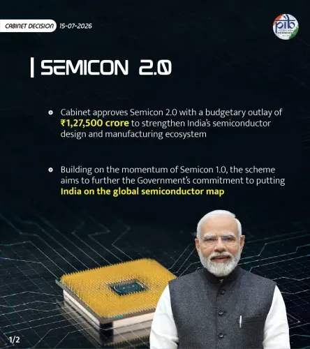
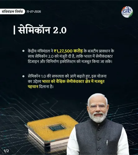
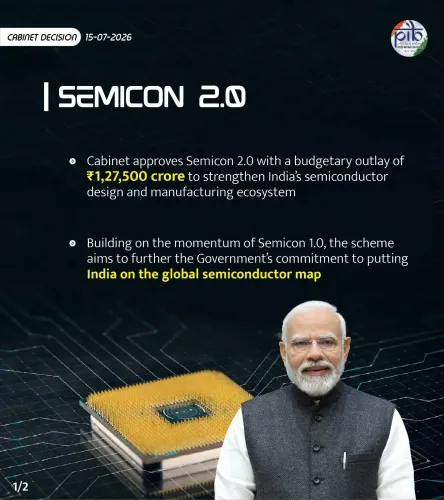
The Union Cabinet has approved Semicon 2.0 with an outlay of Rs 1,27,500 crore, Prime Minister Narendra Modi announced on 15 July 2026. The programme expands on the original 2021 Semicon India scheme and aims to establish India as a global centre for semiconductor design, manufacturing, and innovation.
Key Takeaways
The Union Cabinet approved Semicon 2.0 on 15 July 2026 with a total outlay of Rs 1,27,500 crore .
The new programme is a significant scale-up from the original Semicon India scheme approved in December 2021 with an outlay of Rs 76,000 crore .
The policy targets semiconductor design, manufacturing, and innovation , covering the full value chain.
Prime Minister Modi highlighted India's youth as a core driver of the semiconductor ambition.
The initiative aligns with the Atmanirbhar Bharat framework to reduce reliance on East Asian chip supply chains.
Implementation details, disbursement timelines, and new project announcements under the revised outlay are awaited.
Prime Minister Narendra Modi announced on Wednesday, 15 July 2026 that the Union Cabinet has approved Semicon 2.0, a major expansion of India's semiconductor policy, with a financial outlay of Rs 1,27,500 crore — reaffirming the government's long-term commitment to making India a global hub for chip design, manufacturing, and innovation.
Context
Posting on X, Prime Minister Modi said: 'India's semiconductor journey gets even more vibrant! The Cabinet has approved Semicon 2.0 with an outlay of Rs 1,27,500 crore, reaffirming our long-term commitment to making India a global centre for semiconductor design, manufacturing and innovation. Powered by our youth.' The announcement signals a significant escalation in state support for the domestic semiconductor sector.
The outlay of Rs 1,27,500 crore represents a substantial increase over the original Semicon India programme, which the Union Cabinet had approved in December 2021 with an outlay of Rs 76,000 crore. That earlier programme, administered through the India Semiconductor Mission, laid the institutional groundwork for domestic chip fabrication, design, and packaging capabilities.
Policy Backdrop
India's semiconductor push sits within the broader Atmanirbhar Bharat framework, which seeks to reduce dependence on concentrated East Asian supply chains and attract advanced manufacturing investment. The original 2021 programme introduced production-linked incentives for chip design firms, compound semiconductor units, and assembly and test facilities.
Semicon 2.0 appears to build on that foundation by expanding the scale of central funding and widening the policy architecture. The Prime Minister's specific reference to India's youth underscores a parallel emphasis on engineering talent pipelines — a recurring theme in government technology policy that connects semiconductor manufacturing ambitions to skilling and higher education initiatives.
Stakeholders and Impact
The primary beneficiaries of the expanded outlay are expected to include domestic and foreign semiconductor firms seeking incentives to set up fabrication, assembly, test, and design centres in India. Engineering graduates and technical institutions stand to gain from increased industry demand for skilled chip designers and process engineers.
Global chipmakers that have been evaluating India as a manufacturing destination — partly driven by supply-chain diversification pressures following pandemic-era shortages — may find the enhanced financial commitment a stronger signal of policy continuity. State governments that have already signed agreements under the earlier Semicon India programme are also likely stakeholders in how the revised outlay is structured and disbursed.
What's Next
Attention will now turn to the operational details of Semicon 2.0: the disbursement timeline, the specific incentive structures for different segments of the value chain, and whether the revised programme will be accompanied by new international technology partnerships. The government is expected to release a formal scheme notification through the India Semiconductor Mission with eligibility and application guidelines.
Analysts and industry stakeholders will also watch for announcements of fresh fabrication or assembly projects that could be the first beneficiaries under the expanded outlay — a key test of whether the increased financial commitment translates into on-ground investment and job creation in the near term.
Point of View
The government is signalling that the original programme has produced enough momentum — in terms of investor interest and institutional capacity — to justify a second, larger bet. The emphasis on youth in Prime Minister Modi's announcement is politically deliberate, connecting a capital-intensive industrial policy to a jobs and skills narrative that has broader electoral and social resonance. The real test, however, will be whether the expanded outlay accelerates actual fabrication capacity on Indian soil, or whether the bulk of near-term activity remains concentrated in the less capital-intensive design and packaging segments.
NationPress
15 Jul 2026
Frequently Asked Questions
What is Semicon 2.0 and what is its budget?
Semicon 2.0 is the Indian government's expanded semiconductor policy programme, approved by the Union Cabinet with a financial outlay of Rs 1,27,500 crore. It builds on the original Semicon India programme launched in December 2021 and aims to make India a global hub for chip design, manufacturing, and innovation.
How does Semicon 2.0 differ from the original Semicon India programme?
The original Semicon India programme, approved in December 2021, had an outlay of Rs 76,000 crore. Semicon 2.0 raises that commitment to Rs 1,27,500 crore, representing a substantial increase in central government funding for the semiconductor ecosystem.
Who will benefit from Semicon 2.0?
The primary beneficiaries are expected to include domestic and global semiconductor firms setting up design, fabrication, assembly, and test facilities in India, as well as engineering graduates and technical institutions that supply skilled talent to the sector.
What is the India Semiconductor Mission?
The India Semiconductor Mission is the nodal government body established to implement the country's semiconductor policy, overseeing incentive programmes for chip fabrication, design, compound semiconductors, and packaging under the broader Atmanirbhar Bharat framework.
When did PM Modi announce Semicon 2.0?
Prime Minister Narendra Modi announced the Cabinet approval of Semicon 2.0 on Wednesday, 15 July 2026, via a post on X, describing it as a reaffirmation of India's long-term commitment to becoming a global semiconductor centre.