Will PM Modi Attend the HCL-Foxconn Chip Project Ceremony Today?
Synopsis
Prime Minister Modi's participation in the groundbreaking ceremony of the HCL-Foxconn chip project is a significant step towards India's technological self-reliance. This initiative aims to boost innovation, create jobs, and strengthen the semiconductor manufacturing ecosystem in India.
Key Takeaways
Investment of Rs 3,700 crore for the semiconductor facility.
Collaboration between Foxconn and HCL Group .
Focus on mobile and consumer electronics .
Job creation for thousands of professionals.
Support for India's journey towards technological self-reliance .
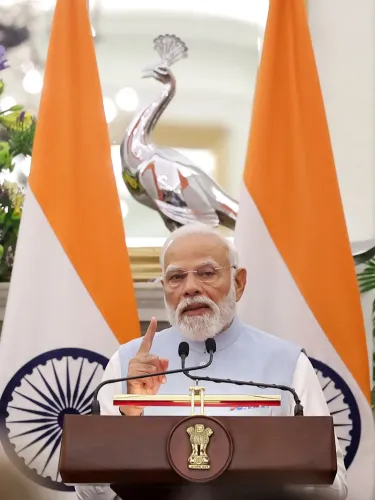
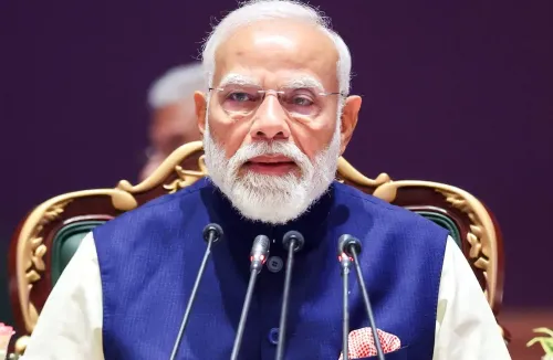
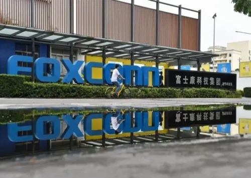
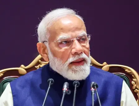
New Delhi, Feb 21 (NationPress) Today, Prime Minister Narendra Modi will participate in the groundbreaking ceremony for the Rs 3,700 crore HCL-Foxconn collaboration project, named India Chip Pvt. Ltd. This event will take place via video conferencing from the Yamuna Expressway Industrial Development Authority (YEIDA) area, located near the Noida International Airport in Jewar, Uttar Pradesh.
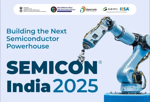
The launch of this semiconductor facility by the Taiwanese electronics titan Foxconn in partnership with India's HCL Group signals a pivotal moment in India’s quest for technological self-sufficiency. It aligns with the Prime Minister’s vision of transforming India into a reliable global hub for high-tech electronics and semiconductor manufacturing.
This Outsourced Semiconductor Assembly and Test (OSAT) facility will be developed under the Modified Scheme for Semiconductor Assembly, Testing, Marking, and Packaging (ATMP) by India Chip Pvt. Ltd., involving an investment exceeding Rs 3,700 crore.
The project is in line with the government’s initiative to enhance domestic manufacturing capabilities, decrease reliance on imports, and cultivate resilient global supply chains.
It is anticipated to significantly impact critical sectors like mobile phones, tablets, laptops, automotive, consumer electronics, and additional devices.
This venture will substantially boost India’s semiconductor ecosystem, promoting innovation, skill development, and technology transfer.
Moreover, the facility is expected to generate numerous direct and indirect job opportunities for engineers, technicians, and professionals, while also stimulating growth in supporting industries.
The HCL-Foxconn collaboration highlights India’s rising prominence in the global semiconductor sector and represents a major advancement in establishing a robust and self-sufficient electronics manufacturing framework.
Foxconn possesses a 40 percent equity stake in this venture and has already invested $37.2 million (approximately Rs 312 crore). The Taiwanese manufacturer may inject up to Rs 424 crore into the company.
YEIDA has designated around 48 acres of land for this project in Sector 28, Jewar, adjacent to the forthcoming Noida International Airport.
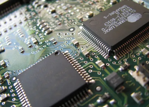
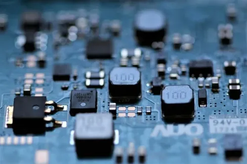
The facility will feature an outsourced semiconductor assembly and testing plant focused on display driver integrated circuits utilized in smartphones, laptops, and automotive applications.
Point of View
I believe that the participation of Prime Minister Modi in this significant project underlines India's commitment to becoming a global leader in semiconductor manufacturing. This initiative not only represents a leap towards technological self-sufficiency but also opens up new avenues for employment and innovation, reinforcing our national interests in the technology sector.
NationPress
3 Jul 2026
Frequently Asked Questions
What is the significance of the HCL-Foxconn project?
The HCL-Foxconn project is crucial for India's technological self-reliance and aims to establish the country as a global hub for semiconductor manufacturing.
How much is being invested in the project?
The project involves a total investment of over Rs 3,700 crore.
What types of products will the facility support?
The facility will support sectors such as mobile phones, tablets, laptops, automotive, and consumer electronics.
How will this project impact employment?
The project is expected to create thousands of direct and indirect job opportunities in various fields.
Where is the project located?
The project is located in the YEIDA area near the Noida International Airport in Jewar, Uttar Pradesh.