Vaishnaw Unveils Semicon 2.0 With ₹1,27,500 Cr Outlay
Synopsis
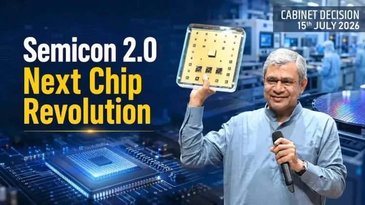
Union Minister Ashwini Vaishnaw has announced Semicon 2.0, a six-pillar semiconductor programme with a ₹1,27,500 crore outlay covering chip design, fabrication, ATMP/OSAT, machines and materials, R&D, and talent development — a major scale-up from India's original 2021 semiconductor mission.
Key Takeaways
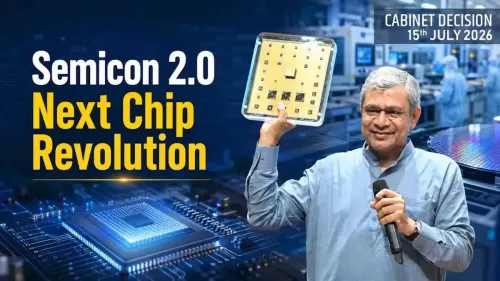
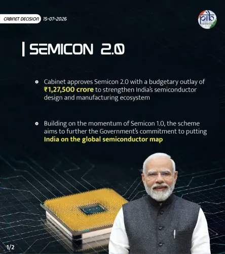
Union Minister Ashwini Vaishnaw announced Semicon 2.0 on 16 July 2026 with a total outlay of ₹1,27,500 crore .
The programme is structured around six pillars : chip design, machines and materials, more fabs, ATMP/OSAT strengthening, R&D, and talent development.
The outlay represents a significant increase from the original India Semiconductor Mission's ₹76,000 crore package approved in December 2021 .
Early projects under the first phase include Micron Technology's ATMP unit in Sanand, Gujarat and Tata Electronics' fab in Assam .
The policy explicitly adds upstream pillars — machines, materials, and talent — not prominently covered in the original mission framework.
Formal disbursement timelines and project approval criteria under the six pillars are awaited via Cabinet or MeitY notifications.
Union Minister Ashwini Vaishnaw announced Semicon 2.0, a revamped semiconductor policy framework carrying a total outlay of ₹1,27,500 crore, on Thursday, 16 July 2026. The programme expands India's chip ambitions across six distinct pillars, signalling a significant scale-up from the original India Semiconductor Mission launched in 2021.
Context
Vaishnaw, who holds the portfolio of Electronics and Information Technology alongside Railways and Information and Broadcasting, outlined the six pillars as: chip design, machines and materials, more fabrication units (fabs), strengthening of assembly, test, mark and pack (ATMP) and outsourced semiconductor assembly and test (OSAT) capacity, research and development, and talent development.
The announcement marks a formal articulation of the government's next-generation semiconductor strategy, building on early project approvals that had already set the foundation for domestic chip manufacturing.
Policy Backdrop
India's semiconductor push began in December 2021 when the Union Cabinet approved the India Semiconductor Mission (ISM) under the Ministry of Electronics and Information Technology (MeitY), with an initial outlay of ₹76,000 crore focused primarily on fabrication incentives, ATMP support, and design-linked schemes.
The first wave of project approvals followed in 2023–24, with Micron Technology receiving clearance for an ATMP facility in Sanand, Gujarat — the first major project under the mission — and Tata Electronics signing agreements for a semiconductor fab in Assam and an ATMP unit in Gujarat in partnership with PSMC of Taiwan.
Semicon 2.0's stated outlay of ₹1,27,500 crore represents a substantial increase over the original package, reflecting the government's intent to move beyond fabrication incentives into upstream design, materials, and human capital — areas that the first phase did not address as explicitly.
Stakeholders and Impact
The six-pillar structure directly addresses gaps identified by industry: India has historically been strong in chip design talent but weak in physical manufacturing infrastructure and the upstream materials and equipment supply chain. By explicitly naming machines and materials as a standalone pillar, the policy signals an intent to build domestic capability in an area currently dominated by a handful of countries.
For engineering graduates and the academic ecosystem, the talent development pillar is particularly significant. The semiconductor sector requires highly specialised skills, and a funded national programme could reshape curriculum priorities at technical institutions.
Electronics manufacturers who depend on imported chips — from consumer electronics to automotive and defence — stand to benefit from a deeper domestic supply chain, potentially reducing import dependence and supply-chain vulnerability.
What's Next
Formal Cabinet or MeitY notifications detailing disbursement timelines, eligibility criteria, and project approval processes under each of the six pillars will be the immediate markers to watch. The annual Semicon India conference has historically served as the primary platform for investment announcements and policy updates in this sector.
India's Semicon 2.0 framework arrives as the United States, European Union, Japan, and Taiwan are each running parallel programmes to diversify semiconductor supply chains away from concentrated East Asian production nodes — positioning India as a potential beneficiary of global friend-shoring trends if implementation timelines hold.
Point of View
Which was heavily weighted toward attracting fabrication plants through fiscal incentives. By codifying six pillars — including machines, materials, and talent — the government is signalling that it understands chip manufacturing as a full-stack challenge, not just a factory-building exercise. The ₹1,27,500 crore outlay, if backed by credible disbursement architecture, would place India among the world's largest state-backed semiconductor programmes by absolute size. The real test will be execution speed: global chipmakers evaluate policy frameworks not on announced outlays but on the predictability and pace of actual incentive disbursements.
NationPress
15 Oct 2026
Frequently Asked Questions
What is Semicon 2.0 in India?
Semicon 2.0 is India's upgraded semiconductor development programme announced by Union Minister Ashwini Vaishnaw on 16 July 2026, with a total outlay of ₹1,27,500 crore structured across six pillars including chip design, fabrication, ATMP/OSAT, machines and materials, R&D, and talent development.
What is the total outlay of Semicon 2.0?
The total outlay of Semicon 2.0 is ₹1,27,500 crore, as announced by Union Minister Ashwini Vaishnaw on 16 July 2026.
What are the six pillars of Semicon 2.0?
The six pillars of Semicon 2.0 are: chip design, machines and materials, more fabrication units (fabs), strengthening of ATMP/OSAT capacity, research and development, and talent development.
How is Semicon 2.0 different from the original India Semiconductor Mission?
The original India Semiconductor Mission, launched in December 2021 with an outlay of ₹76,000 crore, focused primarily on fabrication incentives and ATMP support. Semicon 2.0 expands the scope significantly to ₹1,27,500 crore and adds upstream pillars such as machines and materials and a dedicated talent development pillar.
Which companies have already invested under India's semiconductor mission?
Micron Technology received approval for an ATMP facility in Sanand, Gujarat, and Tata Electronics signed agreements for a semiconductor fab in Assam and an ATMP unit in Gujarat — both under the first phase of the India Semiconductor Mission.