ASML EUV China rumour exposes real lithography gap for chipmakers
Synopsis
ASML's flat denial of EUV shipments to China — prompted by a US commerce secretary's concern — is being ridiculed for logistical implausibility, yet it spotlights a genuine and widening technology gap: Chinese chipmakers are increasingly boxed in as both EUV and advanced DUV access tighten simultaneously.
Key Takeaways
ASML has categorically denied shipping any EUV lithography system or related components to China , following reported concern from US Secretary of Commerce Howard Lutnick .
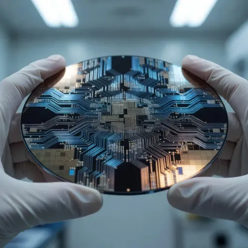
A single ASML EUV machine weighs approximately 180 tonnes and requires large cargo aircraft and specialist installation teams, making covert transfer highly implausible.
Chinese foundries including Semiconductor Manufacturing International Corporation (SMIC) are attempting to compensate through DUV multi-patterning, though analysts note significant yield and cost challenges.
Huawei Technologies is pursuing a system-level approach called Tau Law , while the broader industry explores advanced packaging as alternatives to cutting-edge lithography nodes.
Domestic Chinese lithography tool development continues but remains well behind the capabilities of ASML and Japan 's Nikon .
Export controls on advanced DUV equipment are also tightening, further narrowing the options available to Chinese chipmakers.
ASML has categorically denied shipping any EUV (extreme ultraviolet) lithography system — or components specifically designed for one — to China, after US Secretary of Commerce Howard Lutnick reportedly raised concerns that such technology may have reached the country. The episode, while widely ridiculed by industry observers, cuts to a deeper and more consequential question: with EUV firmly out of reach and access to advanced DUV (deep ultraviolet) tools tightening, how far can Chinese chipmakers realistically go?
Why the rumour was met with ridicule
The logistics alone make an illicit EUV transfer almost impossible to conceal. A single ASML EUV lithography system weighs approximately 180 tonnes, comprises a vast number of precision components, and is typically transported in the cargo holds of large freight aircraft. Installation, calibration, and ongoing service support require teams of specialists — making any covert shipment extraordinarily difficult to execute without detection.
That context is why Secretary Lutnick's reported concern was greeted with scepticism, and in some quarters outright mockery, by semiconductor industry analysts and observers. ASML, headquartered in the Netherlands, has maintained strict compliance with export control regimes that bar it from selling EUV systems to Chinese customers.
The real bottleneck: lithography access
Despite the implausibility of the rumour, the broader issue it surfaces is entirely real. Lithography — the process of etching circuit patterns onto silicon — remains one of the most critical chokepoints in China's semiconductor ambitions. Semiconductor Manufacturing International Corporation (SMIC) and other domestic foundries are attempting to push DUV multi-patterning techniques further than previously thought viable, compensating for the absence of EUV by layering multiple exposure steps.
At the same time, domestic tool makers are working to develop indigenous lithography systems, though these remain well behind the capabilities of ASML and Japan's Nikon. Export controls have also progressively tightened around advanced DUV equipment, narrowing the workaround options available to Chinese fabs.
Alternative paths and their limits
China's chip industry is exploring several parallel strategies to navigate the restrictions. Advanced packaging — stacking and interconnecting chips to boost system-level performance without requiring the most advanced nodes — has gained traction. Huawei Technologies has also been developing its own framework, referred to as Tau Law, as a system-level optimisation approach aimed at extracting greater efficiency from existing process nodes.
Kirin chipsets, produced in partnership with SMIC, have demonstrated that DUV-based multi-patterning can yield competitive results at certain nodes — but analysts, including those at SemiAnalysis, note the yield costs and complexity involved make scaling these approaches economically challenging. TSMC and Samsung Electronics, by contrast, continue to advance on EUV-enabled nodes that remain inaccessible to their Chinese counterparts.
What's next
The ASML denial may close this particular chapter, but the structural tension it highlights will not dissipate. As US export controls evolve and domestic Chinese alternatives remain years behind the frontier, the lithography gap is likely to widen before it narrows. Watch for further tightening of DUV equipment rules and the pace of China's domestic lithography development as the key indicators of how this constraint plays out.
Point of View
Not just EUV. Washington's export control architecture is quietly closing the DUV workaround that Chinese foundries have relied on, which means the multi-patterning bridge that SMIC built to produce Kirin chips could itself become a dead end. What mainstream coverage often misses is that the bottleneck is not a single machine — it is the entire ecosystem of chemicals, optics, metrology tools, and service contracts that surround it, most of which are also subject to allied export controls. The strategic question for 2026 and beyond is not whether China gets EUV, but whether its domestic alternatives can mature fast enough to prevent a node gap from becoming a permanent structural disadvantage.
NationPress
24 Jun 2026
Frequently Asked Questions
Did ASML ship EUV lithography machines to China?
ASML has categorically denied shipping any EUV lithography system, or components specifically designed for one, to China . The denial came after US Secretary of Commerce Howard Lutnick reportedly raised concerns about such a transfer.
Why is it so hard to secretly ship an ASML EUV machine?
An ASML EUV lithography system weighs approximately 180 tonnes and must be transported in large cargo aircraft before undergoing extensive installation and calibration by specialist teams. The scale and complexity make any covert shipment extremely difficult to conceal, which is why industry observers greeted the concern with scepticism.
What is the difference between EUV and DUV lithography?
EUV (extreme ultraviolet) and DUV (deep ultraviolet) refer to different wavelengths of light used to etch circuit patterns onto silicon wafers. EUV uses a much shorter wavelength, enabling the production of more advanced, densely packed chips — and it remains inaccessible to Chinese foundries under current export controls.
How are Chinese chipmakers coping without EUV access?
Chinese foundries such as SMIC are pushing DUV multi-patterning techniques further to approximate more advanced nodes without EUV . Concurrently, Huawei Technologies is developing a system-level optimisation framework called Tau Law , and the industry is investing in advanced packaging as an alternative path to higher performance.
Which companies are most affected by China's lithography restrictions?
Semiconductor Manufacturing International Corporation (SMIC) and other domestic Chinese foundries are most directly constrained, as they cannot access the EUV tools used by rivals TSMC and Samsung Electronics . Huawei Technologies , which relies on domestically produced chips for its Kirin series, is also significantly exposed to any further tightening of DUV equipment export controls.