Prinano claims NIL tech mass-produces optical chips without ASML tools
Synopsis
Hangzhou start-up Prinano claims it has mass-produced photonic chips on 8-inch wafers using nanoimprint lithography — completely bypassing ASML's banned DUV tools — at one-tenth the cost, a potentially significant workaround for China's chip sector.
Key Takeaways
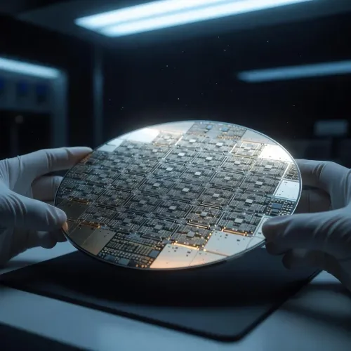
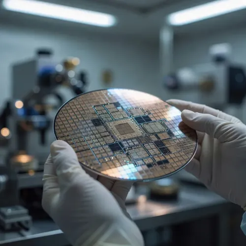
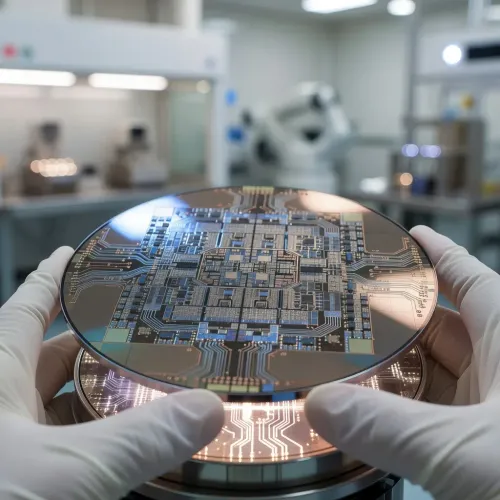
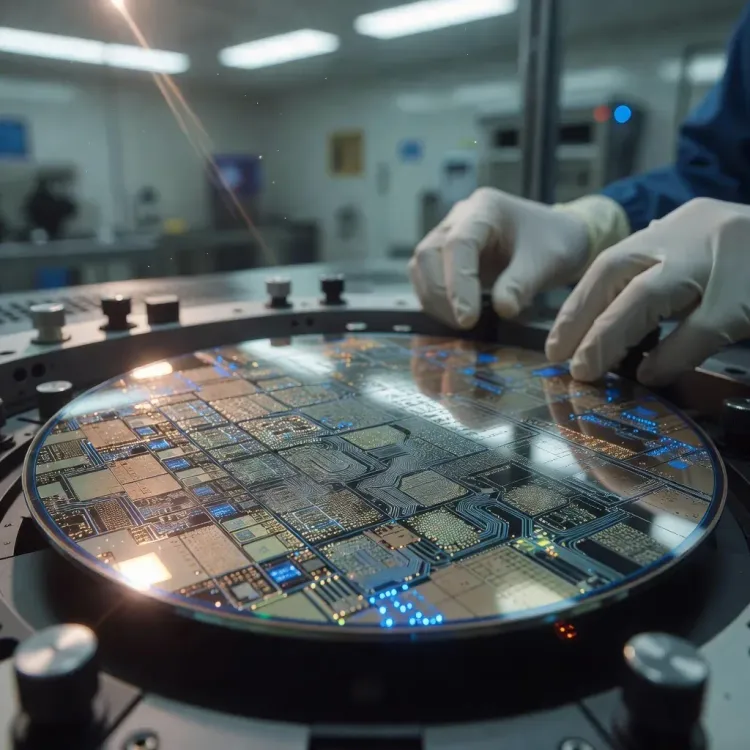
Prinano , based in Hangzhou, Zhejiang province , announced on Friday, 6 June 2026 that it has validated mass production of photonic chips using nanoimprint lithography (NIL) on 8-inch silicon wafers .
The company claims its PL-AS vacuum air-cushion NIL equipment eliminates the need for deep ultraviolet (DUV) lithography tools, which are subject to export bans to China by ASML .
Production costs are reportedly reduced to approximately one-tenth of conventional DUV-based chip manufacturing.
Prinano partnered with Shenzhen Litra Technology to produce the wafers, targeting applications in optical communication, sensing, and lidar .
In August 2025 , Prinano had delivered what it described as China's first semiconductor NIL system to a domestic customer.
Industry analysts, including those at SemiAnalysis , have flagged unresolved questions around NIL's yield, volume scalability, and applicability beyond photonic chips.
Hangzhou-based start-up Prinano says it has successfully validated mass production of photonic chips on 8-inch silicon wafers using nanoimprint lithography (NIL) — entirely bypassing conventional deep ultraviolet (DUV) lithography equipment — at roughly one-tenth the cost of traditional methods. The announcement, made via the company's WeChat account on Friday, 6 June 2026, marks a potential inflection point for China's chip manufacturing sector amid tightening export controls on Western semiconductor tools.
The Technology Behind the Claim
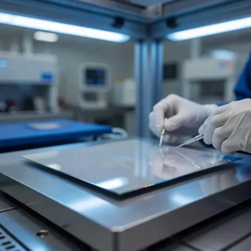
Prinano said it collaborated with Shenzhen Litra Technology to produce the 8-inch optical chip wafers, using the company's proprietary PL-AS vacuum air-cushion nanoimprint lithography equipment. The process relies on what the company described as 'customised double-layer imprinting materials and core processes', according to its official statement. The approach, the company claimed, supports wafer-level production of photonic chips used widely in optical communication, sensing, and lidar applications.
Why It Matters: The ASML Export Ban Context
The development carries strategic weight because both DUV machines and the more advanced extreme ultraviolet (EUV) systems from Dutch chipmaking equipment giant ASML are currently banned from export to China. A domestic alternative — even a partial one — could ease pressure on Chinese chip fabricators locked out of leading-edge lithography tools. Prinano had previously, in August 2025, delivered what it called China's first semiconductor NIL system to a domestic customer, signalling an early commercial push in this space.
The Competitive Backdrop
Nanoimprint lithography is not a new concept — Canon of Japan has long pursued NIL for certain chip applications, and the technique was pioneered in academic settings including Princeton University in the US. However, scaling NIL for high-volume semiconductor manufacturing has historically faced challenges around throughput, yield, and defect rates. Industry analysts and firms such as SemiAnalysis have noted ongoing debate over NIL's real-world viability beyond niche photonic use cases, particularly for logic chips where precision tolerances are far more demanding.
What's Next
The key questions now centre on whether Prinano can demonstrate consistent yields and production volumes at commercial scale — metrics the company has not yet disclosed publicly. The photonic chip segment, while narrower than logic or memory, is strategically critical given its role in AI data centre interconnects, autonomous vehicles, and 5G infrastructure. If the cost and scalability claims hold under independent scrutiny, the technology could attract significant attention from domestic foundries and government-backed chip initiatives alike. Observers will be watching for third-party validation and any customer announcements from Shenzhen Litra Technology in the months ahead.
Point of View
Making optical chips, with their more forgiving tolerances, the most credible near-term use case. What mainstream coverage often misses is that a cost-reduction claim of one-tenth means little without published yield data — in chipmaking, cheap-but-defective is commercially worthless. The more consequential signal here is institutional: if government-backed foundries begin qualifying NIL for photonic lines, it validates a parallel supply chain that could gradually reduce China's vulnerability in specific, strategically important chip categories.
NationPress
23 Oct 2026
Frequently Asked Questions
What has Prinano claimed about its nanoimprint lithography technology?
Prinano claims it has validated mass production of photonic chips on 8-inch silicon wafers using its PL-AS vacuum air-cushion nanoimprint lithography (NIL) equipment, completely bypassing the need for deep ultraviolet (DUV) lithography tools. The company says this approach cuts chip manufacturing costs to roughly one-tenth of conventional DUV-based methods.
Why is this significant for China's semiconductor industry?
Both DUV and more advanced EUV machines from ASML are currently banned from export to China , restricting domestic chipmakers' access to leading-edge lithography. A viable domestic NIL alternative, even for niche photonic applications, could reduce reliance on restricted foreign equipment and support China's chip self-sufficiency goals.
What are photonic chips used for?
Photonic chips are semiconductor devices that use light rather than electrical signals to transmit data. They are widely used in optical communication networks, sensing systems, and lidar — the latter being critical for autonomous vehicles and robotics — as well as in high-speed interconnects inside AI data centres .
Has nanoimprint lithography been proven for mass chip production before?
NIL is an established research and niche manufacturing technique, with companies like Canon of Japan and academic institutions including Princeton University in the US having explored it for years. However, scaling NIL to high-volume, high-yield semiconductor production has historically been challenging, and analysts at firms such as SemiAnalysis have noted ongoing debate over its real-world viability beyond photonic use cases.
What is Prinano's track record in this space?
Prinano , headquartered in Hangzhou, Zhejiang province , delivered what it described as China's first semiconductor NIL system to a domestic customer in August 2025 . The latest announcement, made in partnership with Shenzhen Litra Technology , represents the company's first publicly claimed demonstration of wafer-level mass production using the technology.