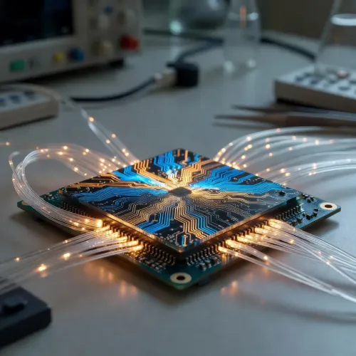
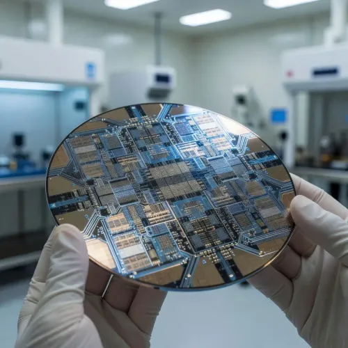
CAS team cuts 3D optical chip build time from hours to seconds
Synopsis
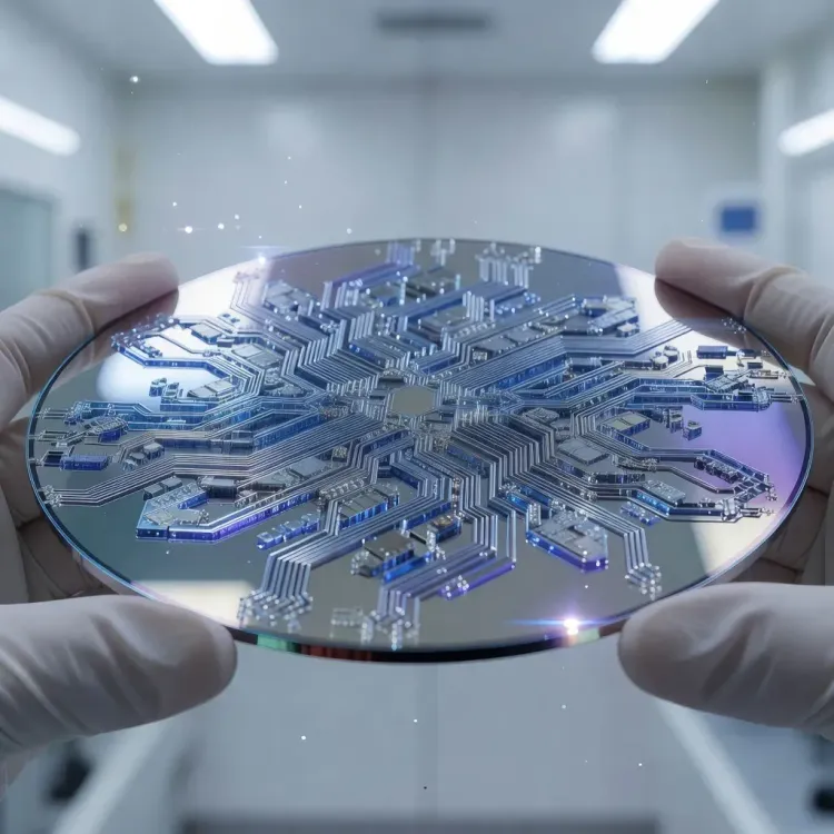
Scientists at China's Institute of Physics under CAS have cut 3D optical structure fabrication time from hours to seconds, a potential inflection point for mass-producing photonic chips that could redefine AI compute hardware supply chains globally.
Key Takeaways
A team led by CAS Institute of Physics PhD student Wang Yi published a new 3D photonic chip fabrication method in Advanced Materials on July 4, 2026 .
The technique reduces production time for complex three-dimensional optical structures from hours to seconds .
Collaborators include scientists from the University of Hong Kong and multiple other Chinese institutions.
The research targets scalable manufacturing for next-generation 3D integrated photonics , a key AI hardware technology.
Global competitors including Intel , Lightmatter , Ayar Labs , NTT , Huawei , Imec , and TSMC are all active in the photonic chip race.
A Chinese Academy of Sciences (CAS) research team has slashed the fabrication time for complex three-dimensional (3D) optical structures from hours to seconds, a breakthrough that could accelerate the path to mass-producible photonic chips for AI hardware. The findings were published in the peer-reviewed journal Advanced Materials on July 4, 2026, and were led by scientists from CAS's Institute of Physics alongside collaborators from the University of Hong Kong and several other Chinese institutions.
Why it matters
Photonic chips transmit data using light rather than electricity, making them a leading candidate to overcome the bandwidth and power constraints that increasingly bottleneck conventional AI compute. The global race to build next-generation AI hardware — involving players such as Intel, Lightmatter, Ayar Labs, NTT, Huawei, and research consortia including Imec and TSMC — has placed photonics at the centre of semiconductor strategy.
Yet a persistent barrier has been manufacturing complexity: producing intricate 3D photonic structures at scale has historically demanded time-consuming, multi-step processes. The new method, according to the research team, directly addresses that bottleneck.
The breakthrough explained
The study, led by PhD student Wang Yi, introduces a fabrication platform designed to bridge the gap between design complexity and scalable production. 'Our work establishes a versatile platform that bridges the gap between design complexity and scalable manufacturing for next-generation 3D integrated photonics,' the team wrote in the paper.
By compressing production time from hours to seconds for complex optical structures, the method could significantly reduce per-unit costs and enable higher manufacturing throughput — two prerequisites for commercial viability in AI chip supply chains.
Competitive backdrop
China has been intensifying investment in photonic and advanced semiconductor research as part of a broader push to develop domestic alternatives to leading-edge chips amid ongoing export controls. CAS, as the country's premier state research body, has increasingly positioned photonics as a strategic priority. Internationally, Japan's NTT and US-based startups like Lightmatter and Ayar Labs are pursuing similar optical interconnect and photonic compute strategies, underscoring the global competitive intensity in this space.
The involvement of the University of Hong Kong as a collaborator also highlights the continued role of Hong Kong academic institutions in mainland-led advanced research programmes.
What's next
The research team's platform is described as 'versatile,' suggesting potential applicability across multiple photonic device architectures beyond the specific structures demonstrated. Whether the technique can be integrated into existing semiconductor fabrication lines — and at what yield — will determine its near-term commercial relevance.
Industry observers will be watching whether CAS or its commercial partners file patents or announce pilot production agreements, as the gap between laboratory demonstration and foundry-scale deployment remains the critical test for any photonic manufacturing advance.
Point of View
Japanese telecoms giants, and now a well-funded Chinese state research apparatus. What mainstream coverage often underplays is the manufacturing gap — dozens of photonic chip designs have been demonstrated in labs over the past decade, but almost none have achieved the throughput needed for AI data-centre volumes. If the CAS method holds up under independent replication and translates to foundry conditions, it could give Chinese photonics an unexpected process-level advantage precisely when export controls are pushing Beijing to accelerate domestic semiconductor alternatives. The collaboration with the University of Hong Kong also signals that cross-border academic ties remain a quiet but significant channel for advanced research, even amid broader geopolitical friction.
NationPress
18 Oct 2026
Frequently Asked Questions
What did the Chinese Academy of Sciences photonic chip team achieve?
Scientists from CAS's Institute of Physics , in collaboration with the University of Hong Kong and other institutions, developed a fabrication method that reduces production time for complex 3D optical structures from hours to seconds. The findings were published in the journal Advanced Materials on July 4, 2026 .
Why does faster photonic chip fabrication matter for AI?
Photonic chips use light instead of electricity to transmit data, offering a path around the bandwidth and power limits that constrain conventional AI processors. Faster fabrication directly lowers cost and raises throughput, the two barriers that have historically prevented photonic technologies from reaching commercial AI hardware at scale.
Who led the photonic chip research?
The study was led by PhD student Wang Yi at the Institute of Physics under the Chinese Academy of Sciences (CAS) , with collaborators from the University of Hong Kong and several other Chinese research institutions.
How does this compare to global photonic chip competitors?
Companies and organisations including Intel , Lightmatter , Ayar Labs , NTT , Huawei , Imec , and TSMC are all pursuing photonic chip technologies. The CAS breakthrough is notable because it targets the manufacturing scalability problem that has stalled many competing photonic programmes.
What happens next after this photonic chip discovery?
The immediate test is whether the fabrication platform can be integrated into existing semiconductor foundry lines at commercial yield levels. Patent filings and any pilot production announcements from CAS or its commercial partners will be the key indicators of how quickly this laboratory result could translate into deployable AI hardware.