Biwin Storage bets $672M on advanced packaging in Dongguan
Synopsis
Biwin Storage Technology is pouring $672 million into a single phase of its Dongguan advanced packaging facility — more than it spent on the first two phases combined — as Chinese storage firms race to master wafer-level chip operations still far from generating mass production revenue.
Key Takeaways
Biwin Storage Technology is investing 4.5 billion yuan (US$672 million) in the third phase of its advanced packaging and testing project in Dongguan, Guangdong , disclosed in a stock filing on 23 September 2026 .
The third-phase investment alone exceeds the combined 3.09 billion yuan spent on the first two phases of the same facility.
The Dongguan facility had not yet generated mass production revenue as of the filing date, remaining in customer sampling and process verification stages.
Biwin targets monthly wafer capacity of 10,000 wafers at the Dongguan site by the end of 2027 , more than tripling current output.
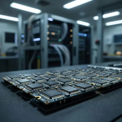
The move represents a shift from Biwin 's existing SiP and traditional memory packaging base in Huizhou , where it relies on externally sourced chips.
Peers including Shenzhen Longsys Electronics and Shenzhen Techwinsemi Technology are pursuing similar advanced packaging upgrades across China .
Biwin Storage Technology, a Shanghai-listed Chinese memory firm, is investing 4.5 billion yuan (US$672 million) in the third phase of its advanced packaging and testing facility in Dongguan, Guangdong province, marking one of the most significant moves by a Chinese storage maker into wafer-level chip operations. The announcement, disclosed in a stock exchange filing on Tuesday, 23 September 2026, signals a broader industry push by Chinese storage companies to climb the semiconductor value chain beyond traditional module assembly.
A bet that dwarfs earlier investments
The 4.5 billion yuan commitment to the third phase alone exceeds the combined 3.09 billion yuan Biwin spent across the first two phases of the same project, according to the company's stock filing. That scale underscores the urgency with which Chinese storage firms are pursuing higher-margin, more technically complex operations. The Dongguan facility is positioned as the centrepiece of Biwin's ambitions in wafer-level packaging — a domain that commands greater pricing power and strategic relevance than downstream module assembly.Why it matters
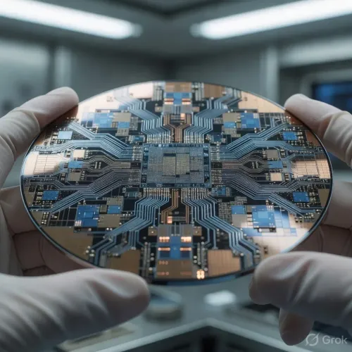
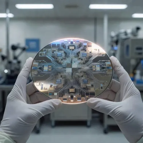
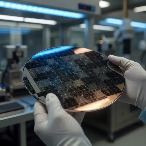
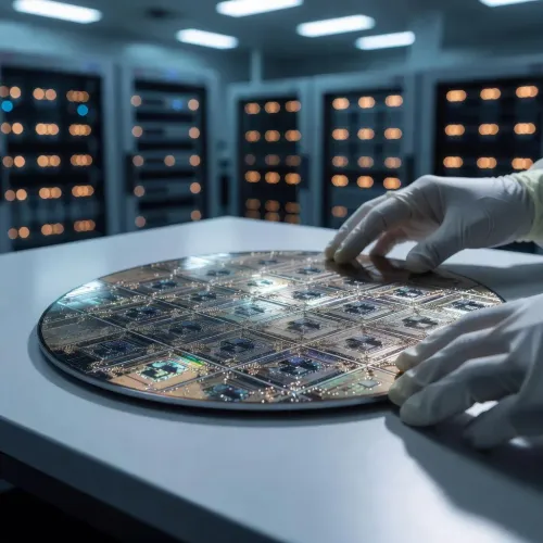
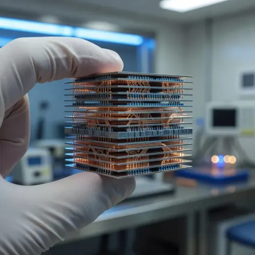
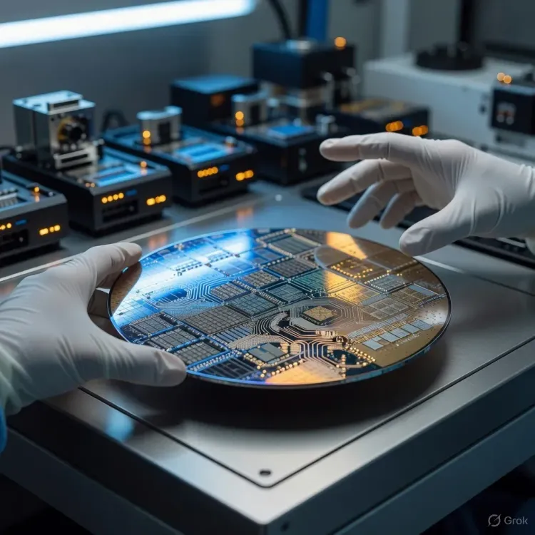
Wafer-level packaging sits closer to the front end of chip manufacturing, requiring more precise process control and deeper engineering capability than conventional system-in-package (SiP) or module work. Biwin already operates a traditional memory and SiP packaging base in Huizhou, also in Guangdong, where it sources chips from external suppliers. The Dongguan project represents a deliberate step toward greater vertical integration and technological self-sufficiency — themes that resonate across China's semiconductor industry amid ongoing export restrictions.Production still in early stages
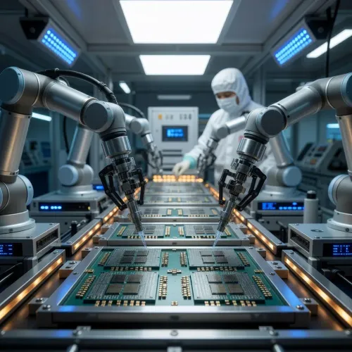
Despite the heavy capital outlay, the Dongguan facility — including its first two phases — had not yet generated mass production revenue as of the filing date, according to the company. The project remains in customer sampling, process verification, and small-batch production stages. Biwin estimated, based on the filing and earlier investor meetings, that the facility's monthly wafer capacity would more than triple to 10,000 wafers by the end of 2027.The competitive backdrop
Biwin is not alone in this pivot. Other Shenzhen- and Jiangsu-based storage players, including Shenzhen Longsys Electronics and Shenzhen Techwinsemi Technology, have been making parallel moves into advanced packaging, according to industry reports. Analysts at Yole Group have flagged China's advanced packaging sector as one of the fastest-growing segments in global semiconductor manufacturing, driven partly by restricted access to leading-edge logic chips and partly by surging domestic AI infrastructure demand.What's next
The critical milestone to watch is whether Biwin can convert customer sampling into volume production contracts before 2027, when the tripled capacity is expected to come online. Failure to secure anchor customers during the verification phase could leave significant capital idle. Investors and industry observers will be monitoring whether the company's wafer-level ambitions translate into recurring revenue — or remain a costly, long-horizon bet in a market still dominated by Samsung, SK Hynix, and Micron.Point of View
Chinese firms are racing to dominate the packaging layer where they can still compete and add margin. What mainstream coverage tends to underplay is the revenue gap: the facility has yet to produce at commercial scale, meaning this is a high-conviction, long-payback bet made under geopolitical pressure rather than demand certainty. The 10,000-wafer-per-month target by end-2027 is achievable on paper, but securing the anchor customers — likely domestic AI server and storage system builders — before that capacity lands will determine whether this is a strategic masterstroke or an expensive placeholder. The broader pattern is clear: advanced packaging is becoming the new front line of China's semiconductor self-sufficiency drive, and Biwin is staking a disproportionate share of its balance sheet on winning it.
NationPress
23 Sept 2026
Frequently Asked Questions
What is Biwin Storage Technology investing in?
Biwin Storage Technology is investing 4.5 billion yuan (US$672 million) in the third phase of an advanced packaging and testing facility in Dongguan, Guangdong province, China . The investment targets wafer-level chip packaging operations, a more technically sophisticated tier than the company's existing module and SiP assembly work.
Why is Biwin's Dongguan investment significant?
The third-phase outlay exceeds the combined 3.09 billion yuan spent on the first two phases, signalling a major escalation in ambition. It positions Biwin among a wave of Chinese storage companies attempting to move up the semiconductor value chain into higher-margin, wafer-level operations amid restricted access to advanced foreign chips.
When will Biwin's Dongguan facility reach full capacity?
Biwin estimates the Dongguan facility will reach a monthly capacity of 10,000 wafers by the end of 2027 , more than tripling its current output. As of the September 2026 filing, the facility — including its first two phases — had not yet generated mass production revenue.
Which other Chinese companies are investing in advanced chip packaging?
Shenzhen Longsys Electronics and Shenzhen Techwinsemi Technology are among the Chinese storage firms making parallel moves into advanced packaging. Industry analysts at Yole Group have identified China 's advanced packaging sector as one of the fastest-growing segments in global semiconductor manufacturing.
How does advanced packaging differ from what Biwin currently does?
Wafer-level advanced packaging sits closer to the front end of chip manufacturing and requires more precise process engineering than conventional module assembly or system-in-package ( SiP ) work. Biwin currently operates a traditional memory and SiP packaging base in Huizhou, Guangdong , where it sources chips from external suppliers rather than processing wafers directly.