Fudan University's single-electron chip could end AI memory bottleneck

Synopsis
A Fudan University team has built a chip called Guiyi that stores one bit of data with a single electron — versus 200,000 in today's best DRAM — and amplifies the signal tenfold, potentially enabling full AI models on mobile phones at near-zero power.
Key Takeaways
Fudan University professor Zhou Peng and colleagues published the Guiyi single-electron 2D flash memory chip in Science on July 16, 2026 .
Today's leading DRAM chips from Samsung and SK Hynix require approximately 200,000 electrons per bit; Guiyi requires just one .
The device boosts the single-electron signal from tens of millivolts to 0.5 volts — a tenfold gain over any prior single-electron memory.
The technology could allow large language models to run on mobile phones with minimal power consumption, according to the research team.
The work was funded by the National Natural Science Foundation of China , underlining state-level strategic interest.
Fudan University researchers in Shanghai have demonstrated a working two-dimensional (2D) flash memory chip that stores data using just one electron — collapsing a figure that stands at roughly 200,000 electrons in today's most advanced DRAM chips from Samsung and SK Hynix. The breakthrough, published on July 16 in the journal Science, could fundamentally reshape how artificial intelligence workloads are handled on low-power devices.
The device and what it does
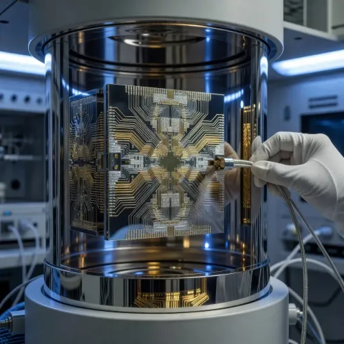
The chip, named Guiyi, was developed by microelectronics professor Zhou Peng and his colleagues at Fudan University. It traps and reads a solitary electron at room temperature — a capability long considered the theoretical ceiling of semiconductor miniaturisation. Critically, Guiyi amplifies the faint signal produced by a single electron from just tens of millivolts to a robust 0.5 volts, representing a tenfold improvement over any previous single-electron memory attempt.
Why it matters for AI
Current DRAM technology requires approximately 200,000 electrons per bit to maintain reliable data storage — a design constraint that drives both the physical size and energy consumption of memory chips. By reducing that count to one, the Guiyi device reaches the absolute theoretical floor for charge-based storage. According to the research team, the most immediate real-world impact would be enabling large language models to run on mobile phones using minimal power, without the AI losing context during extended conversations.
The competitive backdrop
The announcement arrives as global chipmakers race to overcome the memory bandwidth constraints that throttle AI inference at the edge. Samsung and SK Hynix have invested heavily in high-bandwidth memory (HBM) stacks to feed data-hungry AI accelerators, but those solutions are power-intensive and expensive. A viable single-electron memory could render that architectural approach less dominant over time. The research was supported by the National Natural Science Foundation of China, signalling state-level priority for the work.
What's next
Moving from a laboratory demonstration to a manufacturable process node remains a substantial engineering challenge. The 2D material platform underpinning Guiyi must prove compatible with existing semiconductor fabrication lines before commercial timelines can be discussed. Nonetheless, publication in Science — one of the world's most selective peer-reviewed journals — lends the findings significant credibility and will likely accelerate follow-on research globally. Analysts and chipmakers will be watching closely to see whether Fudan University's team can demonstrate yield and endurance metrics consistent with mass production.
Point of View
But the gap between a peer-reviewed laboratory device and a production-ready memory node is where most semiconductor breakthroughs stall. What mainstream coverage underweights is the geopolitical dimension: with US export controls cutting Chinese chipmakers off from leading-edge lithography, China's research institutions are increasingly pivoting to material-science shortcuts — 2D semiconductors, photonic computing, neuromorphic architectures — that could sidestep the conventional scaling roadmap entirely. If Guiyi's signal-amplification approach proves manufacturable, it would threaten the multi-billion-dollar HBM investment thesis that currently underpins SK Hynix's and Samsung's AI-era valuations. The story to watch is not the chip itself but whether Fudan's fabrication partners can demonstrate endurance and yield data within the next 18 months.
NationPress
22 Oct 2026
Frequently Asked Questions
What is the Guiyi chip and who made it?
Guiyi is a two-dimensional flash memory chip developed by professor Zhou Peng and his team at Fudan University in Shanghai . It stores one bit of data using a single electron and was described in a paper published in Science on July 16, 2026 .
Why does single-electron memory matter for AI?
Single-electron memory reaches the theoretical minimum for charge-based data storage, dramatically reducing the power needed to hold information. According to the research team, this could allow large language models to run on mobile phones without losing conversational context — something current memory technology makes impractical.
How does Guiyi compare to Samsung and SK Hynix DRAM?
Today's most advanced DRAM from Samsung and SK Hynix uses roughly 200,000 electrons per bit to maintain reliable storage. Guiyi uses one, and amplifies the resulting signal from tens of millivolts to 0.5 volts — a tenfold improvement over previous single-electron attempts.
When will single-electron memory chips be commercially available?
No commercial timeline has been announced. The Guiyi device is a laboratory demonstration, and scaling a 2D material -based process to mass production involves significant fabrication challenges that remain unsolved.
Who funded the Guiyi single-electron memory research?
The research was supported by the National Natural Science Foundation of China , indicating that the project carries strategic national priority alongside its academic significance.