PM Modi Launches ₹22,516 Crore Semiconductor Facility in Sanand

Synopsis
Prime Minister Modi is set to inaugurate a cutting-edge semiconductor ATMP facility in Sanand, a significant move for India's semiconductor manufacturing ambitions. With a massive investment and a growing workforce, this project is crucial for the future of technology in India.
Key Takeaways
Inauguration of a ₹22,516 crore facility by PM Modi.
Facility developed by Micron Semiconductor Technology .
Focus on assembly, testing, marking, and packaging of memory products.
Current workforce of 2,000 employees , expected to grow to 5,000 .
Significant implications for Artificial Intelligence technologies.
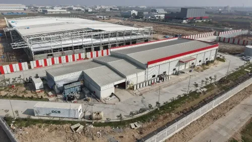
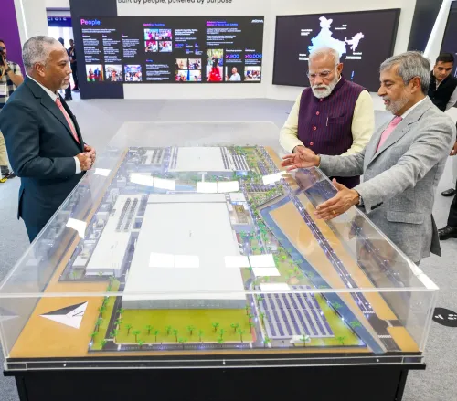
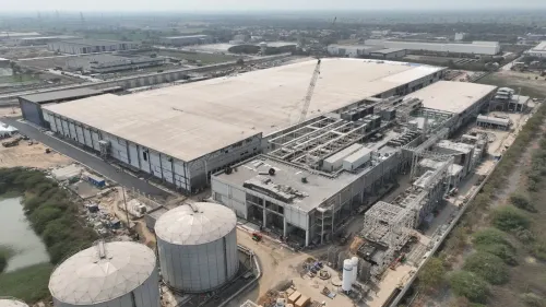
New Delhi, Feb 28 (NationPress) Today, Prime Minister Narendra Modi will unveil a state-of-the-art semiconductor Assembly, Testing, Marking and Packaging (ATMP) facility in Sanand. This inauguration represents a pivotal advancement in India’s aspirations for semiconductor manufacturing, aligning with the National Semiconductor Mission.
The Sanand facility, developed by Micron Semiconductor Technology India Pvt. Ltd., has been established with a hefty investment of Rs 22,516 crore.
This facility will be responsible for the assembly, testing, marking, and packaging of semiconductor memory products, such as solid-state drives (SSDs) and DRAM and NAND devices intended for the global marketplace.
Currently, a dedicated team of 2,000 employees is operational at the plant, with plans to expand the workforce to approximately 5,000 in the coming years.
Notably, individuals with disabilities are also part of the workforce, contributing as operators and technicians, with opportunities available for skilled candidates.
The project has adhered to its scheduled timeline, and officials from the state government have proclaimed that Gujarat is positioning itself as a leader in semiconductor manufacturing within India.
According to Sanjay Mehrotra, President and CEO of Micron Technology, memory and storage are essential in emerging technologies. He stated, "In today’s tech-driven age, especially concerning Artificial Intelligence, memory and storage are vital components. Without robust memory and storage, AI systems cannot operate effectively."
He further noted that as AI applications demand quicker and real-time responses, the need for advanced memory solutions is on the rise.
The semiconductor manufacturing process begins with sand, from which pure silicon is derived. This silicon is then melted and formed into cylindrical ingots and sliced into thin wafers.
At fabrication facilities, intricate electronic patterns are printed onto the wafers, layered through photolithography, which establishes transistors and memory structures.
Subsequently, the wafers are segmented into individual chips, which are sent to the ATMP facility in Sanand for assembly, followed by performance and reliability testing, including evaluations of speed and memory capacity.
After passing tests, the chips are marked and packaged for distribution.
The Sanand unit is set to process advanced DRAM and NAND wafers produced at the company's global factories, converting them into market-ready memory products.
The company has announced that its output will serve international markets and meet the increasing demand for memory and storage solutions, particularly for Artificial Intelligence applications.
Point of View
Positioning Gujarat as a leader in the semiconductor industry.
NationPress
21 Jun 2026
Frequently Asked Questions
What is the significance of the semiconductor facility in Sanand?
The facility represents a crucial step in enhancing India's semiconductor manufacturing capabilities, supporting the National Semiconductor Mission and the growing demand for advanced memory solutions.
Who developed the Sanand semiconductor facility?
The facility has been developed by Micron Semiconductor Technology India Pvt. Ltd. with an investment of ₹22,516 crore.
How many employees currently work at the Sanand facility?
Currently, there are about 2,000 employees at the facility, with plans to increase this number to around 5,000 in the future.
What types of products will be produced at the facility?
The facility will focus on the assembly, testing, marking, and packaging of semiconductor memory products, including SSDs and DRAM and NAND devices.
How does this facility impact the job market?
It will create significant employment opportunities, including roles for individuals with disabilities, contributing to the local economy.