Cabinet Clears Semicon 2.0 With ₹1,27,500 Cr Outlay
Synopsis
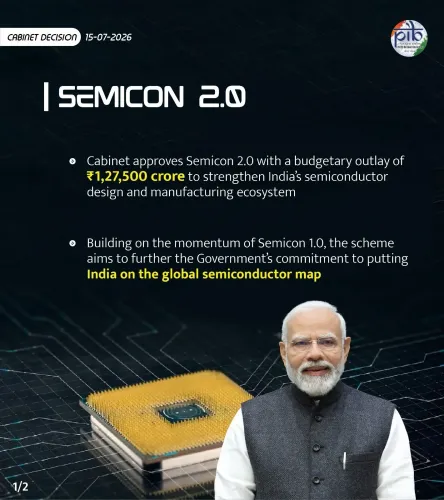
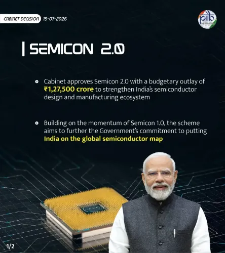
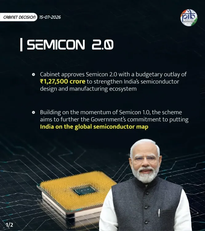
The Union Cabinet has approved Semicon 2.0 with a ₹1,27,500 crore outlay, building on the original Semicon India programme to advance chip design, manufacturing, R&D, talent development and supply chain resilience, as announced by Union Minister Pralhad Joshi on 15 July 2026.
Key Takeaways
The Union Cabinet approved Semicon 2.0 on 15 July 2026 under Prime Minister Narendra Modi .
The budgetary outlay is ₹1,27,500 crore , approximately 67 per cent larger than the ₹76,000 crore allocated under Semicon 1.0 in 2021.
The programme covers chip design, manufacturing, R&D, talent development and supply chain resilience .
The initiative is aimed at positioning India as a global semiconductor hub .
Implementation will be anchored by MeitY and the India Semiconductor Mission , with detailed scheme notifications expected next.
The move aligns with Atmanirbhar Bharat goals and global efforts to diversify semiconductor supply chains.
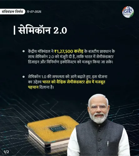
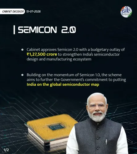
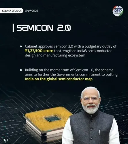
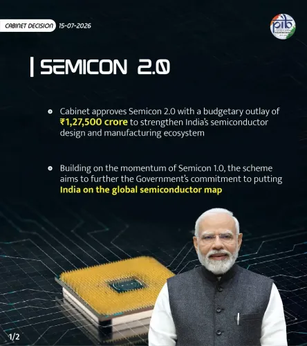
The Union Cabinet, chaired by Prime Minister Narendra Modi, on Wednesday, 15 July 2026, approved Semicon 2.0 — a landmark semiconductor initiative carrying a budgetary outlay of ₹1,27,500 crore — to deepen India's chip design, manufacturing, and supply chain capabilities. Union Minister Pralhad Joshi announced the decision on social media, describing it as building on the foundation laid by the earlier Semicon 1.0 programme.
Context
In his post, Joshi stated that the Cabinet approval would 'boost chip design, manufacturing, R&D, talent development and supply chain resilience, positioning India as a global semiconductor hub.' The announcement comes under the broader #CabinetDecisions series, signalling a formal policy commitment rather than a ministerial proposal. The scale of the outlay — roughly 67 per cent larger than the predecessor programme — underscores the government's accelerating ambition in the sector.
Policy Backdrop
India's semiconductor push has its roots in the India Semiconductor Mission (ISM), launched in 2021 under the Ministry of Electronics and Information Technology (MeitY), which anchored the original Semicon India programme with an outlay of ₹76,000 crore. That first phase targeted attracting fabrication, assembly, testing, marking and packaging (ATMP) investments through production-linked and design-linked incentive schemes. Semicon 2.0 is positioned as the successor, extending incentives deeper into R&D and domestic talent pipelines while addressing supply chain vulnerabilities exposed by global chip shortages in recent years.
India's semiconductor ambitions also sit within the wider Atmanirbhar Bharat framework championed by Prime Minister Modi since 2020, which seeks to reduce the country's dependence on imported electronics components. Geopolitically, the move aligns with efforts by several democracies to diversify semiconductor supply chains away from concentration in East Asia amid ongoing US-China technology tensions.
Stakeholders and Impact
The primary beneficiaries of Semicon 2.0 span a wide industrial arc: domestic chip designers, global fabrication companies considering India as an investment destination, electronics original equipment manufacturers (OEMs), and academic institutions involved in semiconductor research. The talent development component is particularly significant — India currently produces a large pool of engineering graduates but lacks specialised semiconductor design and fabrication training at scale.
For the broader electronics industry, a stronger domestic chip ecosystem could reduce input costs and lead times, making Indian-assembled devices more competitive in both domestic and export markets. Supply chain resilience — explicitly named in the Cabinet decision — addresses a vulnerability that cost Indian electronics manufacturers dearly during the 2020-22 global chip shortage.
What's Next
Attention will now shift to MeitY and the India Semiconductor Mission for detailed scheme notifications spelling out eligibility criteria, incentive structures, and timelines under the ₹1,27,500 crore envelope. Industry observers will watch for announcements of specific fabrication project approvals, memoranda of understanding with international technology partners, and the rollout of talent development programmes linked to the new outlay. The Cabinet decision marks the political commitment; the implementation architecture will determine whether India can translate the investment into tangible manufacturing capacity within the decade.
Point of View
27,500 crore represents the single largest discrete semiconductor policy commitment India has made, signalling that the government views chip self-reliance not as an aspiration but as an industrial-policy priority on par with defence manufacturing. The near-doubling of the financial envelope from Semicon 1.0 suggests the first phase generated enough investor interest — and enough geopolitical urgency — to justify a significantly larger bet. Critically, the explicit inclusion of talent development and R&D alongside manufacturing incentives indicates a maturing of the policy from 'attract assembly plants' to 'build a full-stack ecosystem.' Whether that ambition translates into operational fabs and design houses will depend on execution speed, land and power infrastructure, and the government's ability to hold policy continuity across electoral cycles.
NationPress
15 Jul 2026
Frequently Asked Questions
What is Semicon 2.0 and what is its budget?
Semicon 2.0 is a Union Cabinet-approved semiconductor initiative with a budgetary outlay of ₹1,27,500 crore, aimed at strengthening India's chip design, manufacturing, R&D, talent development and supply chain capabilities.
How does Semicon 2.0 differ from Semicon 1.0?
Semicon 1.0, approved in 2021 with an outlay of ₹76,000 crore, focused primarily on attracting fabrication and assembly investments. Semicon 2.0 expands the scope to include R&D and talent development, and carries a significantly larger financial outlay.
Who announced the Semicon 2.0 Cabinet approval?
Union Minister Pralhad Joshi announced the Cabinet approval of Semicon 2.0 on 15 July 2026 via a post on X, attributing the decision to the leadership of Prime Minister Narendra Modi.
Which ministry oversees India's semiconductor mission?
The Ministry of Electronics and Information Technology (MeitY) oversees the India Semiconductor Mission, which is the nodal body for implementing semiconductor incentive schemes including the Semicon programmes.
Why is India investing in semiconductor manufacturing?
India aims to reduce dependence on imported chips, build supply chain resilience, and integrate into global semiconductor value chains — goals that have gained urgency following global chip shortages and ongoing US-China technology tensions.