Rajnath Singh hails Semicon 2.0 with ₹1,27,500 cr outlay
Synopsis
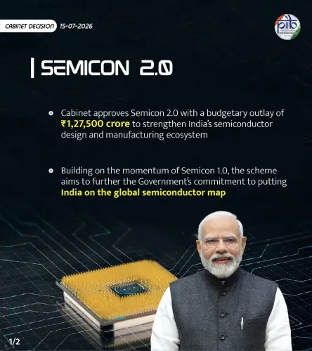
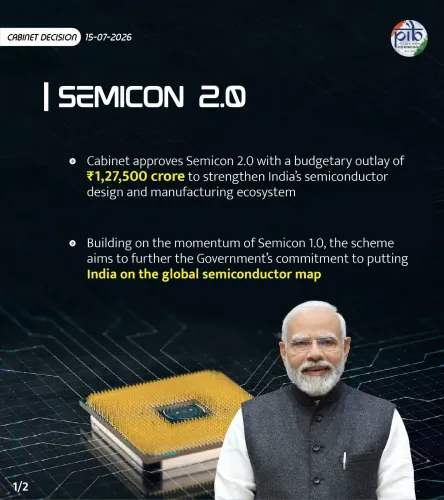
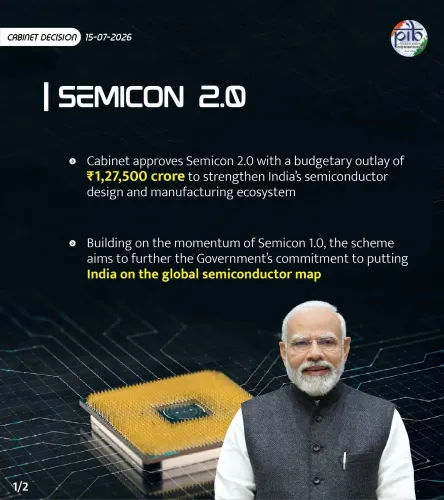
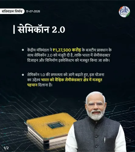
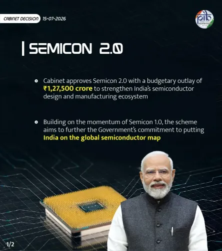
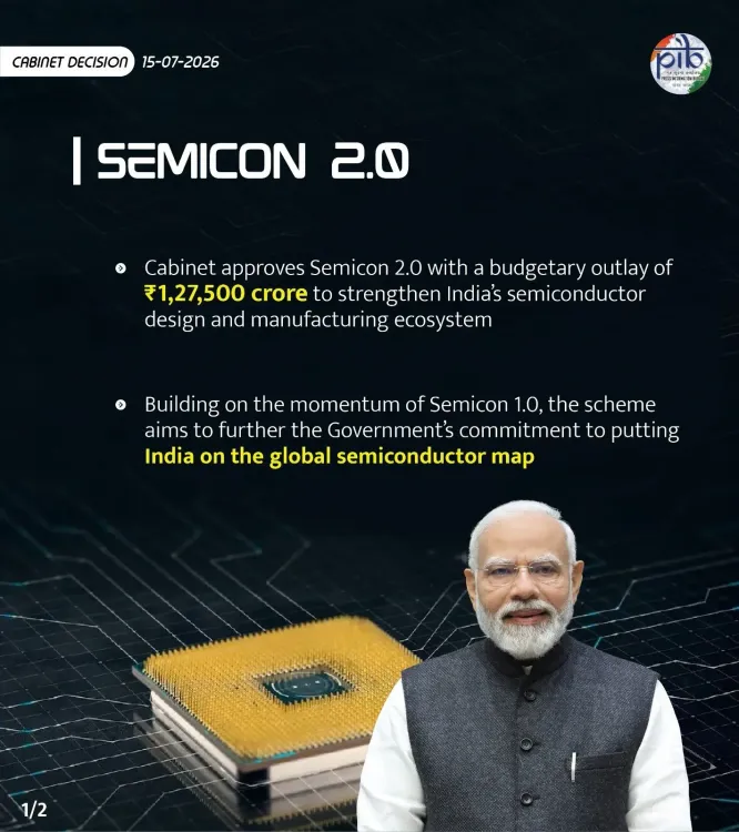
The Union Cabinet chaired by PM Narendra Modi approved Semicon 2.0 on 15 July 2026, committing ₹1,27,500 crore to build India's semiconductor ecosystem across chip design, manufacturing, R&D and talent. Defence Minister Rajnath Singh hailed the decision as a landmark step toward strategic and technological self-reliance.
Key Takeaways
The Union Cabinet approved Semicon 2.0 on 15 July 2026 , chaired by PM Narendra Modi .
The scheme carries a total outlay of ₹1,27,500 crore , roughly 68 per cent higher than the original ₹76,000 crore Semicon India programme approved in December 2021 .
Semicon 2.0 covers chip design, advanced manufacturing, R&D, talent development, and the full semiconductor value chain.
The initiative aims to position India as a trusted global semiconductor hub, with implications for both commercial electronics and defence supply chains.
Union Defence Minister Rajnath Singh credited PM Modi's 'unwavering commitment' to making India a global technology powerhouse.
Detailed scheme guidelines from MeitY and the India Semiconductor Mission are expected to follow the Cabinet approval.
Union Defence Minister Rajnath Singh on Wednesday, 15 July 2026 welcomed the Union Cabinet's approval of Semicon 2.0, a landmark semiconductor policy package carrying an outlay of ₹1,27,500 crore, describing it as a transformative step toward making India a globally competitive chip-manufacturing hub.
Context
Rajnath Singh posted on X that the Union Cabinet, chaired by Prime Minister Narendra Modi, had approved Semicon 2.0, calling it 'a landmark decision that reaffirms India's long-term commitment to building a globally competitive semiconductor ecosystem.' He expressed gratitude to PM Modi for 'his unwavering commitment to making India a global technology powerhouse.'
The announcement marks a significant scaling-up of India's semiconductor ambitions. The minister highlighted that the initiative would strengthen 'chip design, advanced manufacturing, R&D, talent development and the entire semiconductor value chain,' while creating high-value jobs and enhancing technological self-reliance.
Policy Backdrop
The approval builds on a policy lineage that began in December 2021, when the Union Cabinet first approved the Semicon India programme with an outlay of ₹76,000 crore under the India Semiconductor Mission (ISM), administered by the Ministry of Electronics and Information Technology (MeitY). That programme sought to attract semiconductor fabrication, display, and assembly units to India through a combination of fiscal incentives and technology partnerships.
Semicon 2.0's outlay of ₹1,27,500 crore represents a substantial increase — roughly 68 per cent higher than the original programme — signalling the government's intent to move from policy foundation to industrial scale. India has pursued electronics and chip incentives since 2020 to reduce dependence on concentrated East Asian supply chains, a strategic priority amplified by global chip shortages that disrupted automotive, consumer electronics, and defence sectors.
The initiative also sits within the broader Atmanirbhar Bharat framework and complements international technology dialogues such as the initiative on Critical and Emerging Technology (iCET), through which India has sought chip-related cooperation with partner nations.
Stakeholders and Impact
The semiconductor value chain spans a wide range of actors. Domestic and foreign chip design firms, advanced manufacturing units, and assembly, testing, marking and packaging (ATMP) facilities are among the primary beneficiaries of fiscal support under such programmes. Engineering graduates and research institutions stand to gain from the talent-development pillar that Rajnath Singh specifically highlighted.
For the defence sector — which falls directly under Rajnath Singh's portfolio — semiconductor self-sufficiency carries strategic weight. Indigenously sourced chips reduce vulnerability in defence electronics, radar systems, and communication platforms, aligning Semicon 2.0 with the government's broader push for defence indigenisation. India's stated goal of positioning itself as a 'trusted global semiconductor hub' also targets supply-chain partnerships with allied nations seeking to diversify away from geopolitically sensitive sources.
What's Next
Detailed scheme guidelines from MeitY and the India Semiconductor Mission are expected to follow the Cabinet approval, outlining eligibility criteria, incentive structures, and timelines for project applications. Subsequent project-level approvals by the ISM will be the first concrete test of how quickly the expanded outlay translates into on-ground investment commitments.
Any supplementary budget provisions in the next fiscal year and the pace of international technology partnerships will be closely watched as indicators of whether India can convert this policy ambition into a functioning domestic semiconductor industry within the decade.
Point of View
Particularly for defence electronics. The scale of the commitment also reflects competitive pressure from the United States, the European Union, and Japan, all of which have enacted their own chip subsidy regimes. Whether India can attract anchor fabrication investments at this outlay will determine if Semicon 2.0 becomes a turning point or another well-funded aspiration.
NationPress
14 Oct 2026
Frequently Asked Questions
What is Semicon 2.0 India?
Semicon 2.0 is the Union Cabinet's upgraded semiconductor incentive programme approved on 15 July 2026, with a ₹1,27,500 crore outlay to support chip design, advanced manufacturing, R&D, and talent development across India's semiconductor value chain.
What is the outlay for Semicon 2.0?
The Union Cabinet approved Semicon 2.0 with a total outlay of ₹1,27,500 crore, a significant increase over the original Semicon India programme's ₹76,000 crore approved in December 2021.
What did Rajnath Singh say about Semicon 2.0?
Rajnath Singh called the Cabinet's approval 'a landmark decision that reaffirms India's long-term commitment to building a globally competitive semiconductor ecosystem' and expressed gratitude to PM Modi for his commitment to making India a global technology powerhouse.
How does Semicon 2.0 differ from the original Semicon India programme?
The original Semicon India programme, approved in December 2021, had an outlay of ₹76,000 crore. Semicon 2.0 raises that to ₹1,27,500 crore and is expected to expand scope across chip design, manufacturing, R&D, and talent pipelines.
Why is India investing in semiconductor manufacturing?
India is investing in semiconductors to reduce dependence on concentrated East Asian supply chains, support defence electronics indigenisation, create high-value engineering jobs, and position the country as a trusted chip-supply partner for allied nations.