PCB manufacturing push: Vaishnaw, Yogi lay ₹6,750 crore foundation in Jewar
Synopsis
India imports PCBs worth ₹40,000 crore every year — and two new plants in Jewar, backed by ₹6,750 crore in combined investment, are the Centre's direct answer to that drain. With a South Korean JV, Amber Enterprises, and Noida International Airport all converging on the same corridor, Jewar is being positioned as India's next big electronics manufacturing bet.
Key Takeaways
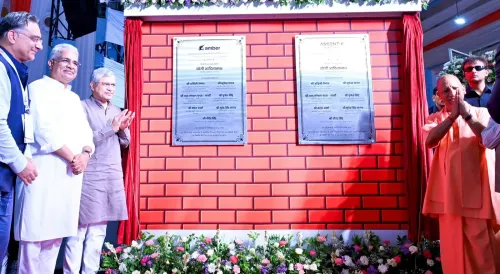
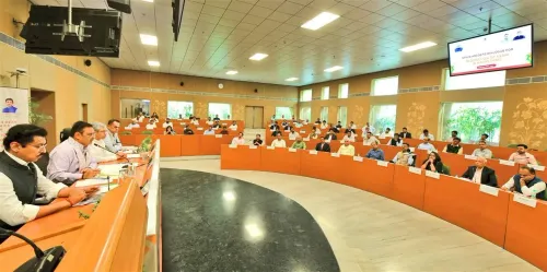
Ashwini Vaishnaw and Yogi Adityanath jointly laid foundation stones for two electronics plants in Yamuna City, Jewar on 28 June .
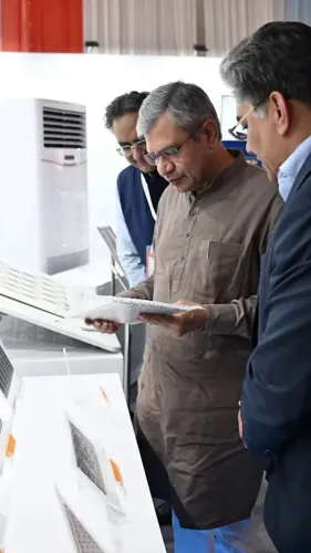
ASCENT-K Circuit , a joint venture with South Korea's KCC , will invest ₹3,250 crore to manufacture high-density and multi-layer PCBs.
Amber Enterprises will invest ₹3,500 crore in a facility for HVAC components and PCB assemblies.
India currently imports PCBs worth nearly ₹40,000 crore annually; domestic production aims to cut this significantly.
Jewar's appeal is underpinned by the Noida International Airport , the DMIC , and the proposed Delhi-Lucknow-Varanasi bullet train project.
Union Minister Ashwini Vaishnaw and Uttar Pradesh Chief Minister Yogi Adityanath on 28 June jointly laid the foundation stones for two major electronics manufacturing facilities in Yamuna City, Jewar, committing a combined investment of ₹6,750 crore toward advanced printed circuit board (PCB) production. The projects are expected to significantly reduce India's dependence on imported PCBs, which currently cost the country nearly ₹40,000 crore annually in foreign exchange.
What the Projects Involve
The first facility, by ASCENT-K Circuit — a joint venture with South Korea's KCC — will invest ₹3,250 crore to manufacture high-density and multi-layer PCBs for the broader electronics industry. The second project, by Amber Enterprises, will deploy ₹3,500 crore to set up a plant producing HVAC components and PCB assemblies. Together, the two facilities represent one of the largest single-location electronics manufacturing commitments in the National Capital Region.
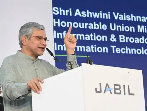
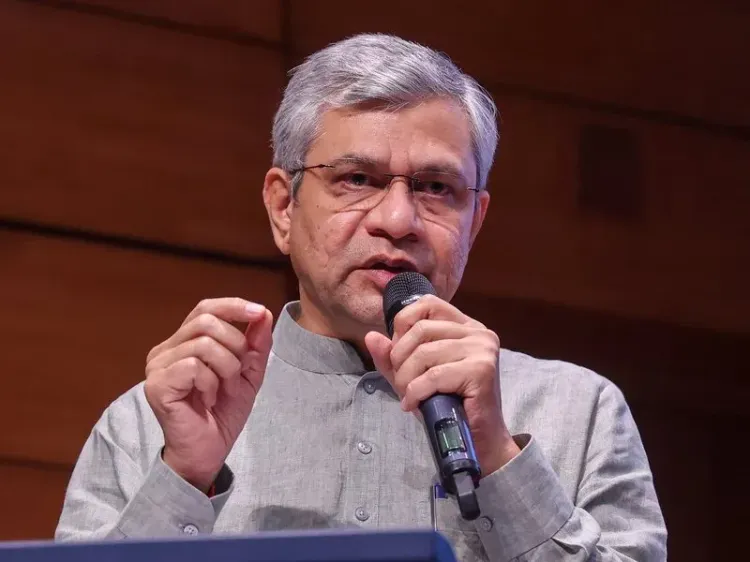
What Vaishnaw Said
Vaishnaw described the development as 'a new chapter in Bharat's electronics manufacturing,' saying in a post on social media platform X that the Amber and Ascent Electronics plants would produce advanced PCBs, 'strengthening India's electronics ecosystem and global competitiveness.' He added: 'Every PCB manufactured here will save foreign exchange, strengthen the rupee and improve India's balance of payments.'
Why Jewar Was Chosen
The minister pointed to the rapidly maturing infrastructure ecosystem around Jewar as a key draw for global investors. He cited the operational Noida International Airport, enhanced connectivity via the Delhi-Mumbai Industrial Corridor (DMIC), and the proposed Delhi-Lucknow-Varanasi bullet train project as factors making the region increasingly attractive. This comes amid a broader Centre-led push to develop Jewar as a multi-modal industrial and logistics hub.
Impact on India's Electronics Ecosystem
India's electronics sector has long been constrained by its reliance on imported PCBs — the foundational component in virtually every electronic device. Domestic PCB manufacturing capacity has historically lagged demand, forcing device makers to source boards from China, South Korea, and Taiwan. The new facilities aim to address that structural gap. Notably, this investment aligns with the Centre's broader semiconductor and electronics localisation agenda, which has seen several incentive frameworks rolled out over the past three years.
Employment and Industrial Outlook
Officials indicated that the projects would generate employment in the Jewar region, though specific job numbers were not announced at the foundation-laying ceremony. The minister said the emerging industrial ecosystem, backed by modern infrastructure, would help position India as a major global electronics manufacturing hub while boosting local production capabilities. Industry observers will watch whether these plants attract further downstream investment from component suppliers and device assemblers into the corridor.
Point of View
000 crore worth of PCBs annually is not a new problem — it has been flagged repeatedly in policy documents since at least 2019. What is new is the scale of private capital now willing to co-locate in a single corridor, partly because Noida International Airport has made Jewar a credible logistics node rather than just a policy aspiration. The real question is whether these plants will anchor a full supply chain — substrate materials, chemicals, laminates — or remain isolated assembly points that still depend on imported inputs. Past electronics clusters in India have struggled to move beyond the final assembly stage. If Jewar can attract upstream suppliers, it changes the calculus; if not, the foreign-exchange savings will be partial at best.
NationPress
28 Jun 2026
Frequently Asked Questions
What are the PCB manufacturing plants being set up in Jewar?
Two facilities are being established in Yamuna City, Jewar: a ₹3,250 crore plant by ASCENT-K Circuit (a joint venture with South Korea's KCC) for high-density and multi-layer PCBs, and a ₹3,500 crore facility by Amber Enterprises for HVAC components and PCB assemblies. Their foundation stones were laid on 28 June by Union Minister Ashwini Vaishnaw and UP Chief Minister Yogi Adityanath.
Why is domestic PCB manufacturing important for India?
India currently imports printed circuit boards worth nearly ₹40,000 crore annually, placing a significant burden on the country's foreign exchange reserves and balance of payments. Domestic production would reduce import dependence and support the broader electronics manufacturing ecosystem.
What infrastructure advantages does Jewar offer for electronics manufacturing?
Jewar benefits from the operational Noida International Airport, connectivity through the Delhi-Mumbai Industrial Corridor (DMIC), and the proposed Delhi-Lucknow-Varanasi bullet train project, making it an attractive destination for domestic and global manufacturing investors.
Who is the South Korean partner in the Jewar PCB project?
The South Korean partner is KCC, which has entered a joint venture with Ascent to form ASCENT-K Circuit. The JV will manufacture high-density and multi-layer PCBs at the ₹3,250 crore Jewar facility.
How do these plants fit into India's broader electronics strategy?
The investments align with the Centre's ongoing push to localise electronics and semiconductor supply chains, reducing reliance on imports from China, South Korea, and Taiwan. PCBs are a foundational component in virtually every electronic device, and domestic capacity is seen as critical to India's ambition of becoming a global electronics manufacturing hub.