Vaishnaw Flags New PCB Plant at Jewar, UP
Synopsis
Union Minister Ashwini Vaishnaw has announced the Amber & Ascent Electronics Manufacturing Plant at Jewar, Uttar Pradesh, which will produce advanced Printed Circuit Boards — a move aimed at reducing import dependence and strengthening India's electronics component ecosystem under existing PLI and SPECS policy frameworks.
Key Takeaways
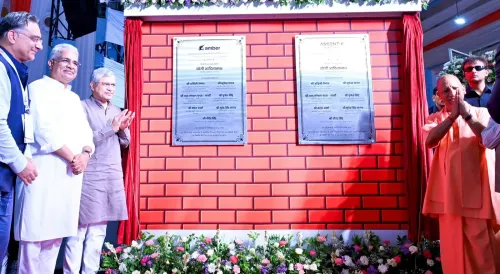
Union Minister Ashwini Vaishnaw announced the Amber & Ascent Electronics Manufacturing Plant at Jewar, Uttar Pradesh on 27 June 2026 .
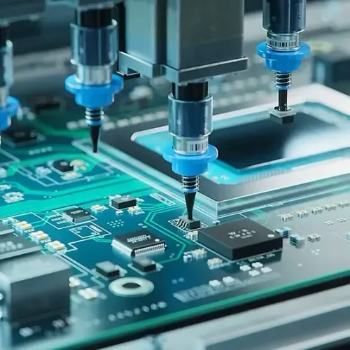
The plant will manufacture advanced Printed Circuit Boards (PCBs) , a critical electronics component segment dominated by imports.
Amber Enterprises , an Indian consumer-durables components company, is expanding into higher-value PCB production through this joint venture.
The facility aligns with the central government's PLI Scheme and SPECS launched in 2020 to deepen domestic electronics manufacturing.
Jewar is part of an emerging industrial corridor in western Uttar Pradesh anchored by the upcoming Noida International Airport .
The plant supports India's strategy to diversify global electronics supply chains and reduce dependence on imported components.
Union Minister Ashwini Vaishnaw on Saturday, 27 June 2026, announced the inauguration of the Amber & Ascent Electronics Manufacturing Plant at Jewar, Uttar Pradesh, marking what he described as 'a new chapter in Bharat's electronics manufacturing.' The facility will produce advanced Printed Circuit Boards (PCBs), a critical component segment where India has historically depended heavily on imports.
Context
PCBs form the backbone of virtually every electronic device, from smartphones and laptops to industrial equipment and defence systems. India's electronics sector has long been characterised by final assembly rather than deep component manufacturing, making PCB production capacity a strategically significant addition. The Jewar location in western Uttar Pradesh is emerging as a major industrial node, anchored by the upcoming Noida International Airport and expanding industrial corridors in the region.
Amber Enterprises, a listed Indian company with roots in components for consumer durables, has been diversifying into higher-value electronics manufacturing. The joint venture with Ascent represents a move further up the value chain into substrate and circuit board production, which demands precision engineering and significant capital investment.
Policy Backdrop
The plant fits squarely within a cluster of central government initiatives launched since 2020 to deepen India's electronics manufacturing base. The Production Linked Incentive (PLI) Scheme for Large Scale Electronics Manufacturing, notified in 2020, extended output-linked financial incentives to domestic and foreign firms investing in the sector. Alongside it, the Scheme for Promotion of Manufacturing of Electronics Components and Semiconductors (SPECS) specifically targeted the component gap — the precise segment a PCB plant addresses.
These schemes sit under the broader Make in India initiative announced in 2014, which identified electronics as a priority sector. The policy architecture has progressively shifted emphasis from attracting assembly operations toward encouraging local value addition in components, materials, and sub-assemblies — a transition that PCB manufacturing directly represents.
Stakeholders and Impact
Uttar Pradesh stands to gain industrial employment and supply-chain linkages as the facility becomes operational. The state has actively positioned its western districts — including Jewar, Greater Noida, and the broader Yamuna Expressway Industrial Development Authority (YEIDA) corridor — as alternatives to saturated manufacturing hubs in other states. Electronics component firms across the country could benefit from a domestic PCB supply source, potentially reducing lead times and foreign-exchange outflows associated with imports.
Global electronics supply-chain diversification pressures, accelerated since 2020, have pushed multinational original equipment manufacturers to seek India-based component suppliers. A domestic PCB manufacturing base strengthens India's pitch to such companies as a credible alternative sourcing destination.
What's Next
Attention will now turn to the ramp-up timeline at the Jewar facility and the production volumes it achieves in its initial phases. Further announcements on component manufacturing clusters in Uttar Pradesh and potential capacity additions by other players in the PCB space are likely to follow as the policy environment continues to incentivise deep manufacturing. The facility's performance will be an early test of whether India's component ambitions can translate into globally competitive output at scale.
Point of View
Strategically sensitive layer of the value chain. For Minister Vaishnaw, who oversees both electronics policy and its implementation, the optics of a domestic PCB facility reinforce the government's narrative of industrial self-reliance ahead of a period when global supply-chain realignment is creating genuine market openings. Uttar Pradesh's positioning as an electronics destination also carries political salience, signalling that industrial investment is reaching states beyond the traditional southern manufacturing belt. Whether this single facility catalyses a broader PCB cluster or remains an isolated milestone will depend on how quickly ancillary suppliers and skilled labour pools develop around it.
NationPress
27 Jun 2026
Frequently Asked Questions
What is the Amber and Ascent Electronics Manufacturing Plant in Jewar?
It is a new manufacturing facility at Jewar in Uttar Pradesh, announced by Union Minister Ashwini Vaishnaw on 27 June 2026, that will produce advanced Printed Circuit Boards (PCBs) to strengthen India's domestic electronics component supply chain.
What are Printed Circuit Boards and why are they important for India?
Printed Circuit Boards are the foundational substrate that connects and supports electronic components in virtually every device. India has historically imported a large share of its PCB requirements, so domestic production capacity reduces import dependence and supports local value addition.
How does the PLI Scheme support PCB manufacturing in India?
The Production Linked Incentive Scheme for Large Scale Electronics Manufacturing, notified in 2020, provides output-linked financial incentives to firms investing in domestic electronics production, making facilities like the Amber & Ascent plant more commercially viable.
Why is Jewar in Uttar Pradesh chosen for electronics manufacturing?
Jewar is part of an emerging industrial corridor in western Uttar Pradesh, supported by the upcoming Noida International Airport and the Yamuna Expressway Industrial Development Authority zone, which offers infrastructure and connectivity advantages for new manufacturing investments.
What is Amber Enterprises' role in Indian electronics manufacturing?
Amber Enterprises is an Indian company originally focused on components for consumer durables that has been expanding into higher-value electronics manufacturing segments, with the Jewar PCB plant representing a move further up the electronics value chain.