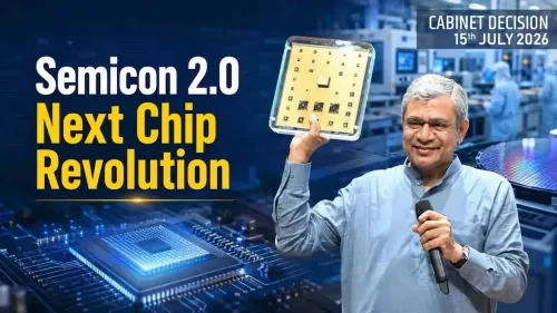
Semicon India 2026: Foundation laid, Semicon 2.0's 6 pillars to drive growth
Synopsis
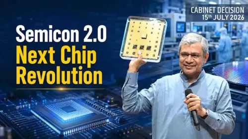
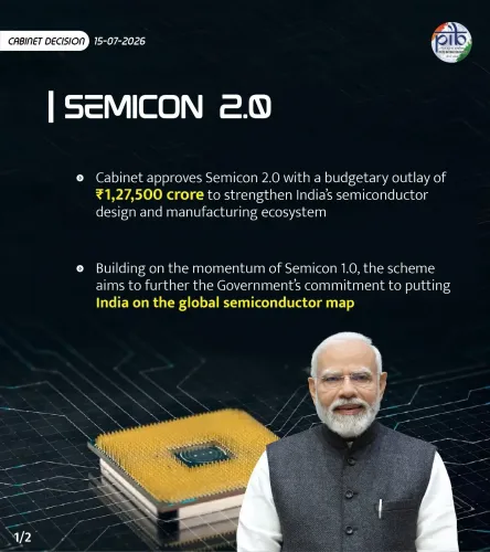
India has moved from semiconductor policy to execution. At SEMICON India 2026, Minister Ashwini Vaishnaw unveiled Semicon 2.0's six-pillar framework — covering fabs, ATMP, design, R&D, materials, and talent — backed by evidence that Semicon 1.0 already seeded 20 VC-funded startups worth ₹800 crore. With 40,000 delegates from 52 countries in attendance, the world is watching India's chip ambitions closely.
Key Takeaways
Union Minister Ashwini Vaishnaw announced that India's semiconductor foundation is set and Semicon 2.0 will drive the next growth phase.
Semicon 2.0 is built on six pillars : Design; Machines and Materials; More Fabs; ATMP/OSAT strengthening; R&D; and Talent Development.
Under Semicon 1.0 , more than 105 startups participated and about 20 secured VC funding of approximately ₹800 crore .
SEMICON India 2026 drew nearly 40,000 delegates from 52 countries and over 600 companies, including 300-plus overseas firms.
Semicon 2.0 projects will run for up to six years ; applications will be accepted for an initial three years , with a mandatory mid-term review.
The India Semiconductor Mission (ISM) will serve as the nodal agency overseeing applications and implementation.
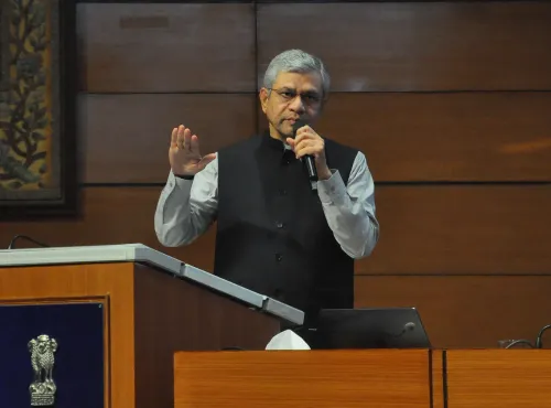
Union Minister for Electronics and IT Ashwini Vaishnaw declared on Thursday, 17 September 2026, that India has successfully laid the foundation of its semiconductor industry and must now accelerate growth across the entire value chain. Speaking on the sidelines of SEMICON India 2026 in New Delhi, the minister outlined a six-pillar framework under Semicon 2.0 as the blueprint for the country's next phase of chip-industry expansion.
Six Pillars of Semicon 2.0
The government has formally notified all six pillars of the Semicon 2.0 scheme, which together cover the full semiconductor value chain. The pillars are: Design; Machines and Materials; Setting up more Fabs; Further strengthening the ATMP/OSAT industry; Research and Development; and Talent Development.
Vaishnaw emphasised a broad domestic ambition, saying, 'whether it is materials, machinery, additional new fabs, ATMP units, design, or talent development — the effort is to develop all of these within India.' The scheme provides fiscal and infrastructure support across every link in the chain, from chip design and fabrication to packaging, equipment, materials, and workforce creation.
Semicon 1.0: The Launchpad
Vaishnaw pointed to concrete early results from the predecessor programme. 'In Semicon 1.0, we had lots of startups trying to see how we can design the chips. We had a good success. More than 105 startups participated in it, and about 20 of them got VC funding of about ₹800 crore. That was just the beginning,' the minister said.
This context matters: Semicon 1.0 was the first structured attempt by India to seed a domestic chip-design ecosystem, and the venture-capital traction achieved by roughly one in five participating startups signals early commercial validation — a prerequisite for the far larger ambitions embedded in the 2.0 iteration.
Scale of SEMICON India 2026
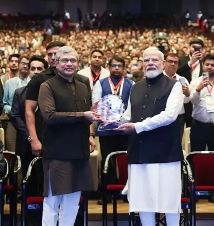
The event itself reflected surging global interest in India as a semiconductor destination. IT Secretary S. Krishnan noted that the conference has grown sharply year on year. 'We have close to about 40,000 delegates registered. We have nearly 600-plus companies participating in the exhibition. We have delegates from about 52 countries participating, and more than 300 of these companies participating in the exhibition are overseas companies. This reflects the kind of confidence that the world has in India as a destination for semiconductor manufacturing,' Krishnan said.
Scheme Structure and Oversight
Projects supported under Semicon 2.0 will generally carry a duration of up to six years, while the scheme will remain open for applications for an initial period of three years. The India Semiconductor Mission (ISM) has been designated as the nodal agency and will handle application intake, technical and financial appraisal, applicant recommendation, and implementation oversight.
A mid-term assessment is mandated after three years of implementation, or earlier if required, to evaluate impact and consider modifications. This built-in review mechanism is a departure from earlier industrial schemes that lacked formal mid-course correction provisions.
What Comes Next
The formal notification of all six pillars marks a pivot from policy design to execution. Industry observers note that the real test will be how quickly fab and ATMP applications are processed and whether talent pipelines — perennially the bottleneck in deep-tech sectors — can be scaled fast enough to meet the demand that new fabs will generate. With global chipmakers reassessing supply-chain concentration in East Asia, India's window to attract anchor investments is arguably narrower than the six-year project horizon suggests.
Point of View
But the distance between a notified scheme and a functioning fab remains vast. The Semicon 1.0 startup numbers are encouraging, yet ₹800 crore in VC funding across 20 companies is seed-stage money in an industry where a single leading-edge fab costs tens of billions of dollars. The six-pillar framework is structurally sound, but talent development — listed last — is arguably the first constraint: without a deep pool of process engineers and materials scientists, new fabs will either stall or import their critical workforce, undermining the 'develop all of these within India' pledge. The mandatory mid-term review after three years is a welcome accountability mechanism, but its teeth depend entirely on whether ISM publishes granular progress data or issues only headline-level assurances.
NationPress
17 Sept 2026
Frequently Asked Questions
What is Semicon 2.0 and what does it cover?
Semicon 2.0 is India's second-generation semiconductor industry development scheme, formally notified by the government in September 2026. It is structured around six pillars — Design, Machines and Materials, Fab expansion, ATMP/OSAT strengthening, R&D, and Talent Development — providing fiscal and infrastructure support across the full chip value chain.
What were the outcomes of Semicon 1.0?
Under Semicon 1.0, more than 105 startups participated in chip-design initiatives, and approximately 20 of them received venture-capital funding totalling around ₹800 crore. Minister Ashwini Vaishnaw described this as 'just the beginning' and the springboard for the more ambitious Semicon 2.0 framework.
How long will Semicon 2.0 projects last and who oversees them?
Projects under Semicon 2.0 will generally run for up to six years, with the scheme open for applications for an initial three-year window. The India Semiconductor Mission (ISM) is the designated nodal agency responsible for receiving applications, conducting appraisals, and overseeing implementation.
How big was SEMICON India 2026 and why does it matter?
SEMICON India 2026 registered close to 40,000 delegates from 52 countries, with over 600 companies — including more than 300 overseas firms — participating in the exhibition. IT Secretary S. Krishnan said the scale 'reflects the kind of confidence that the world has in India as a destination for semiconductor manufacturing.'
What is the mid-term review provision under Semicon 2.0?
A mandatory mid-term assessment is scheduled after three years of implementation, or earlier if needed, to evaluate the scheme's impact and decide on modifications or continuation. This built-in accountability mechanism is designed to allow course corrections before the full six-year project cycle is complete.