Intel, 3D Glass Solutions sign MoU with Odisha for chip packaging facility
Synopsis
Intel and 3D Glass Solutions have signed an MoU with Odisha to explore a glass core semiconductor packaging facility — a move framed as a direct outcome of the Modi-Trump TRUST Initiative agreed in February 2025. If it clears regulatory and funding hurdles, the project could make Odisha an unlikely anchor of India's semiconductor ambitions.
Key Takeaways
Intel Corporation and 3D Glass Solutions signed an MoU with the Odisha government on 1 June 2025 to explore a semiconductor glass core packaging facility.
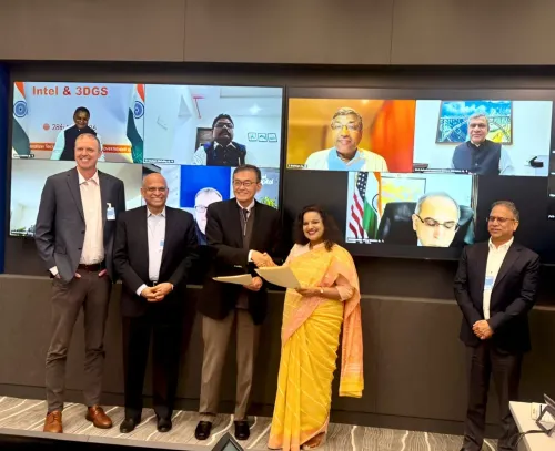
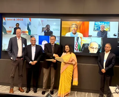
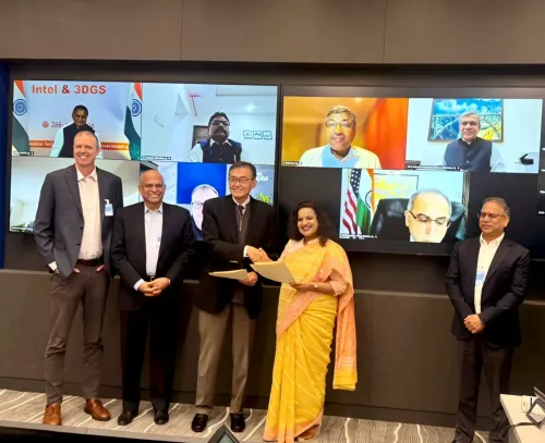
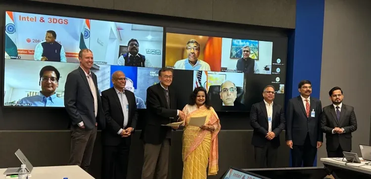
The agreement was signed at Intel's headquarters in Santa Clara, California .
The project is linked to the US-India TRUST Initiative agreed during PM Modi's Washington visit in February 2025 .
The facility, if built, could make Odisha a hub for semiconductor packaging, AI infrastructure, and data centres.
The project remains subject to regulatory approvals and funding support from both state and Central governments.
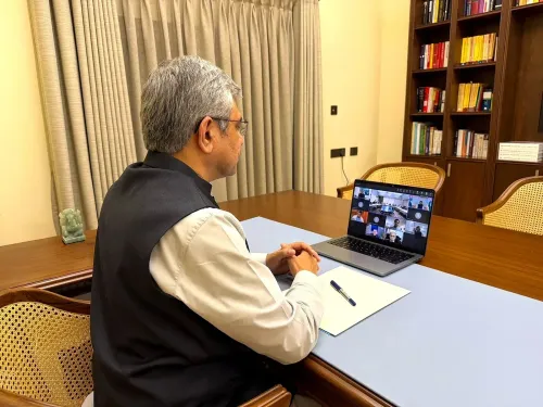
Union IT Minister Ashwini Vaishnaw and Odisha CM Mohan Charan Majhi both endorsed the initiative as aligned with India's manufacturing ambitions.
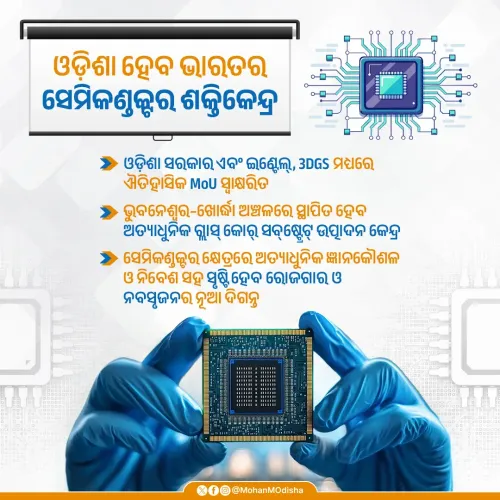
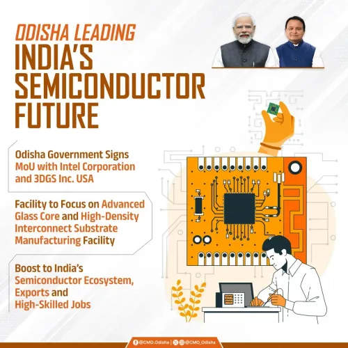
Intel Corporation and 3D Glass Solutions have signed a memorandum of understanding with the Odisha government to explore setting up an advanced semiconductor glass core packaging substrate manufacturing facility in the state — a development that could significantly advance India's ambitions to emerge as a global semiconductor hub.
The MoU was signed at Intel's headquarters in Santa Clara, California, on 1 June 2025, according to a media statement. The agreement is exploratory in nature, with the project still subject to regulatory approvals, funding support from both state and Central governments, and other business conditions.
What the Facility Could Mean for Odisha
If realised, the proposed facility would rank among the largest technology investments in eastern India. Officials and industry leaders say it could position Odisha as an emerging destination for semiconductor manufacturing, advanced packaging, artificial intelligence infrastructure, next-generation data centres, and broader digital technologies.
The scale of ambition is notable: this is not merely a single-product plant but a potential anchor for an integrated technology ecosystem in a state that has historically been associated with steel and mining rather than high-tech manufacturing.
The US-India Technology Diplomacy Angle
India's Ambassador to the United States, Vinay Kwatra, linked the initiative directly to the bilateral technology cooperation framework. He said the MoU advances the vision articulated by Prime Minister Narendra Modi and US President Donald J. Trump during Modi's visit to Washington, D.C. in February 2025.
'This initiative marks an important milestone in advancing the vision articulated by Prime Minister Narendra Modi and President Donald J. Trump during the Prime Minister's visit to Washington, D.C., in February 2025, for collaboration between the two countries in advanced manufacturing under the US-India TRUST (Transforming relationship utilising strategic technology) Initiative,' Kwatra said.
The TRUST Initiative, announced earlier this year, is designed to deepen cooperation between the two countries in semiconductors, telecommunications, and defence technology — areas where both governments have flagged strategic interest.
What the Government Said
Union Electronics and Information Technology Minister Ashwini Vaishnaw said the proposal aligns with India's push to expand domestic manufacturing. 'This initiative reflects India's larger vision of strengthening domestic manufacturing capabilities and positioning the country as a global economic powerhouse,' he said.
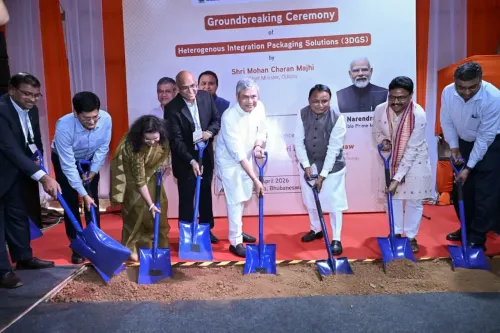
Odisha Chief Minister Mohan Charan Majhi described the development as a turning point for the state. 'Today marks the beginning of a new chapter in Odisha's growth story,' Majhi said, adding that the initiative goes beyond semiconductor manufacturing to encompass AI infrastructure, data centres, and digital transformation. 'Our vision is to build a vibrant ecosystem that inspires future generations, creates world-class opportunities for our youth, attracts leading global technology companies, and firmly places Odisha on the global semiconductor map,' he added.
Industry Voices
Babu Mandava, Chief Executive Officer of 3D Glass Solutions, said the collaboration with Intel and the Odisha government could help establish India as a key global hub for advanced glass substrates and semiconductor packaging, supporting sectors such as artificial intelligence, high-performance computing, and next-generation electronics.
Naga Chandrasekaran, Executive Vice President and General Manager of Intel Foundry, said the company was 'proud to collaborate with 3DGS in exploring this opportunity with the Government of Odisha,' and expressed enthusiasm about accelerating the commercialisation of next-generation advanced packaging solutions globally.
What Happens Next
The MoU is a preliminary agreement, and significant milestones — including regulatory clearances, confirmed funding commitments, and finalised business terms — remain ahead. Analysts note that India's semiconductor ambitions have attracted multiple MoUs in recent years, but converting signed agreements into operational fabs and packaging facilities has proven to be the harder challenge. The Odisha project's progress will be closely watched as a test of whether eastern India can attract advanced technology investment at scale.
Point of View
And India's semiconductor story has accumulated more signed agreements than operational facilities. The Odisha proposal is strategically significant — glass core substrate technology is genuinely next-generation, and Intel's involvement lends credibility — but the conditionalities attached are substantial. Funding support from both state and Central governments is still unconfirmed, and regulatory approvals are pending. The real test is whether this MoU follows the trajectory of Micron's Sanand plant or joins the longer list of semiconductor announcements that stalled between signing and groundbreaking.
NationPress
15 Oct 2026
Frequently Asked Questions
What did Intel and 3D Glass Solutions sign with the Odisha government?
Intel Corporation and 3D Glass Solutions signed a memorandum of understanding with the Odisha government on 1 June 2025 to explore establishing an advanced semiconductor glass core packaging substrate manufacturing facility in the state. The agreement was signed at Intel's headquarters in Santa Clara, California.
What is the US-India TRUST Initiative mentioned in the MoU?
The TRUST Initiative — short for Transforming Relationship Utilising Strategic Technology — is a bilateral framework announced by Prime Minister Narendra Modi and US President Donald J. Trump during Modi's Washington visit in February 2025. It is aimed at deepening cooperation in advanced manufacturing, semiconductors, and defence technology.
Is the Odisha semiconductor facility confirmed?
No. The project remains exploratory and is subject to regulatory approvals, funding support from both the Odisha state government and the Centre, and other business conditions. The MoU is a preliminary agreement to investigate feasibility, not a confirmed investment.
Why is Odisha significant for semiconductor manufacturing?
If the facility is established, it would rank among the largest technology investments in eastern India and could position Odisha as a hub for semiconductor packaging, AI infrastructure, and next-generation data centres — sectors the state has not traditionally been associated with.
What is glass core substrate technology?
Glass core substrate is an advanced semiconductor packaging technology that uses glass instead of traditional organic materials as the base layer for chips. It enables higher performance, better power efficiency, and denser interconnects — making it relevant for AI processors and high-performance computing applications.