CM Majhi: Odisha to Become India's Semiconductor Hub
Synopsis
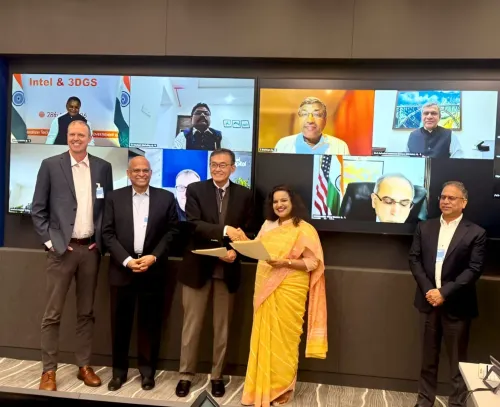
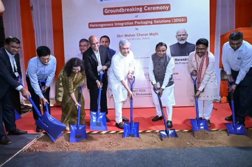
Odisha Chief Minister Mohan Charan Majhi has announced a tripartite MoU between the Odisha government, Intel, and 3DGS for an advanced glass core substrate manufacturing facility in the Bhubaneswar–Khordha corridor, positioning the state as India's semiconductor powerhouse under the national SemiconIndia framework.
Key Takeaways
Odisha government has signed an MoU with Intel and 3DGS (3D Glass Solutions) for semiconductor manufacturing collaboration.
An advanced glass core substrate manufacturing facility is planned for the Bhubaneswar–Khordha industrial corridor.
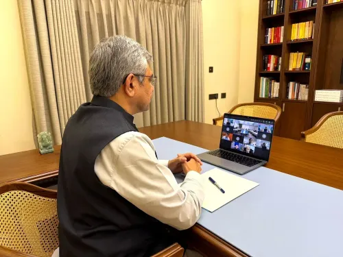
The agreement falls under India's SemiconIndia programme, overseen by Union Minister Ashwini Vaishnaw .
Glass core substrate technology is a next-generation semiconductor packaging frontier that Intel is actively developing globally.
The project is expected to generate employment and attract technology investment, though specific figures have not been disclosed.
Odisha joins Gujarat and Tamil Nadu in positioning itself as a major node in India's emerging semiconductor supply chain.
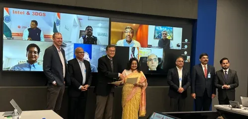
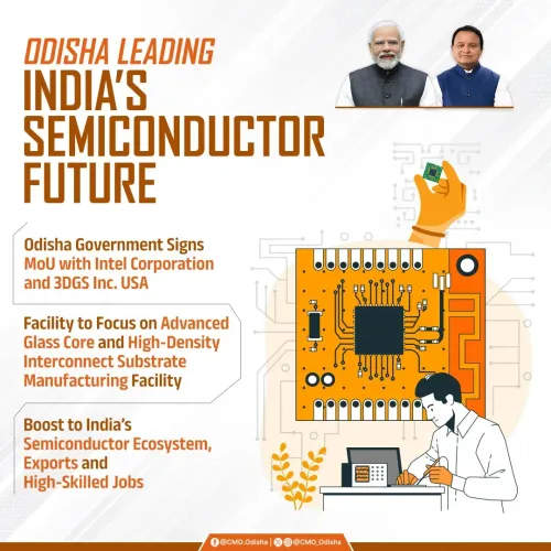
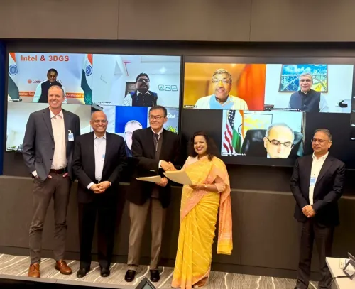
Odisha Chief Minister Mohan Charan Majhi on Monday, June 2, 2026, announced that the Odisha government has signed a Memorandum of Understanding with Intel and 3DGS (3D Glass Solutions), marking what he described as the beginning of a new chapter in the state's industrial and technological development.
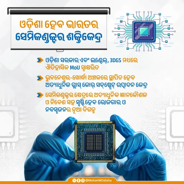
Posting in Odia on X, the Chief Minister declared: 'Odisha heba Bharatara semiconductor shaktikendra' — 'Odisha will become India's semiconductor powerhouse.' He added that the MoU between the Odisha government, Intel, and 3DGS has inaugurated a new era of industrial and technological advancement for the state.
Context
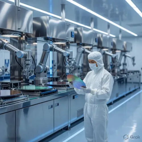
The agreement centres on the establishment of an advanced glass core substrate manufacturing facility in the Bhubaneswar–Khordha corridor. Glass core substrates are a next-generation semiconductor packaging technology that Intel has been developing to replace conventional organic substrates, enabling denser and more power-efficient chip packaging. 3DGS specialises in glass-based substrate and packaging technologies and is positioned as a key technology partner in this venture.
Chief Minister Majhi noted that the facility would place Odisha on the global semiconductor map with a distinct identity, combining cutting-edge technology, large-scale investment, and skilled human resources to generate employment and open new horizons of innovation.
Policy Backdrop
The MoU aligns with India's broader semiconductor self-reliance drive. The India Semiconductor Mission, launched in 2021, provides financial incentives for chip design, fabrication, and advanced packaging. The Production Linked Incentive (PLI) scheme for semiconductors, expanded in 2022–23, has actively courted global firms for assembly, testing, and substrate units.
The SemiconIndia programme, overseen by Union Minister of Electronics and Information Technology Ashwini Vaishnaw — who was tagged in the Chief Minister's post — has been the central framework under which multiple state-level MoUs have been executed since 2024. Odisha's agreement follows a national pattern of eastern and southern states competing to host advanced semiconductor facilities alongside established hubs in Gujarat and Tamil Nadu.
Stakeholders and Impact
The Bhubaneswar–Khordha industrial corridor stands to benefit most directly, with the proposed facility expected to draw electronics manufacturers, engineering talent, and ancillary technology investors to the region. Odisha's engineering workforce and technical institutions are likely to be tapped for the skilled human resources the project requires.
For Intel, the partnership represents an expansion of its India footprint at a time when global chip supply chain diversification is accelerating. The glass core substrate segment is a strategic frontier for the company, and a manufacturing base in Odisha could serve both domestic demand and export supply chains across Asia.
What's Next
The detailed investment scale, employment projections, and operational timeline for the glass core substrate facility have not been disclosed in the post or associated announcements. Official project releases from the Odisha government and the Union Ministry of Electronics are expected to provide specifics on financial commitments and phased rollout.
With Ashwini Vaishnaw and the SemiconIndia programme tagged directly, central government endorsement and potential co-incentivisation under the national semiconductor framework are likely to follow. Further state or central announcements on additional semiconductor projects for Odisha under the SemiconIndia umbrella are anticipated in the coming months.
Point of View
With Odisha leveraging the SemiconIndia framework to attract frontier packaging technology. Chief Minister Majhi's decision to tag Union Minister Ashwini Vaishnaw publicly suggests the state is seeking central co-incentivisation, which would accelerate the project's credibility and funding prospects. Glass core substrate manufacturing is a globally nascent segment, meaning Odisha is not entering a crowded field but staking a claim in an emerging technology niche — a strategically shrewd positioning. The broader implication is that India's semiconductor map is diversifying geographically, reducing concentration risk and expanding the talent and supply chain base across multiple states.
NationPress
18 Oct 2026
Frequently Asked Questions
What is the Intel and Odisha MoU about?
The MoU between the Odisha government, Intel, and 3DGS (3D Glass Solutions) is aimed at establishing an advanced glass core substrate manufacturing facility in the Bhubaneswar–Khordha corridor, positioning Odisha as a semiconductor manufacturing hub.
What is a glass core substrate in semiconductors?
A glass core substrate is a next-generation semiconductor packaging material being developed to replace conventional organic substrates. It enables denser, more power-efficient chip packaging and is a key area of investment for Intel globally.
What is the SemiconIndia programme?
SemiconIndia is India's flagship government initiative to build a domestic semiconductor ecosystem. It provides financial incentives for chip design, fabrication, and advanced packaging, and is overseen by Union Minister of Electronics Ashwini Vaishnaw.
Where will the Odisha semiconductor facility be located?
The proposed glass core substrate manufacturing facility is planned for the Bhubaneswar–Khordha industrial corridor in Odisha.
How does this MoU fit into India's semiconductor policy?
The agreement aligns with the India Semiconductor Mission launched in 2021 and the PLI scheme for semiconductors expanded in 2022–23, both of which incentivise global firms to set up advanced packaging and substrate manufacturing units in India.