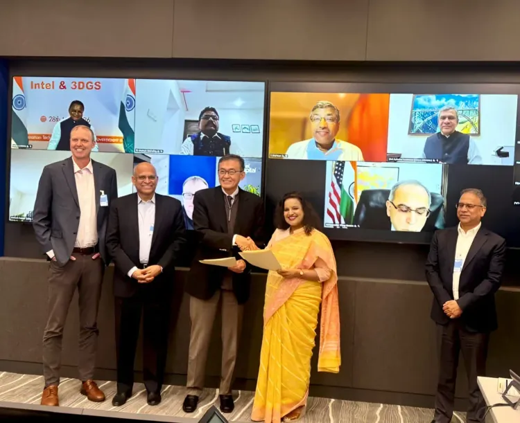
Odisha signs $3.3 billion semiconductor MoU with Intel, 3DGS for India-first facility
Synopsis
Odisha has landed a $3.3 billion semiconductor deal that no other Indian state has — a glass-based advanced packaging facility backed by Intel, the first of its kind in the country. In a global race to diversify chip supply chains away from Taiwan and China, this MoU puts Bhubaneswar on the map for a technology segment that is rapidly becoming the new frontier of semiconductor manufacturing.
Key Takeaways
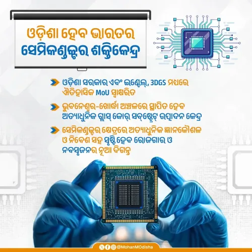
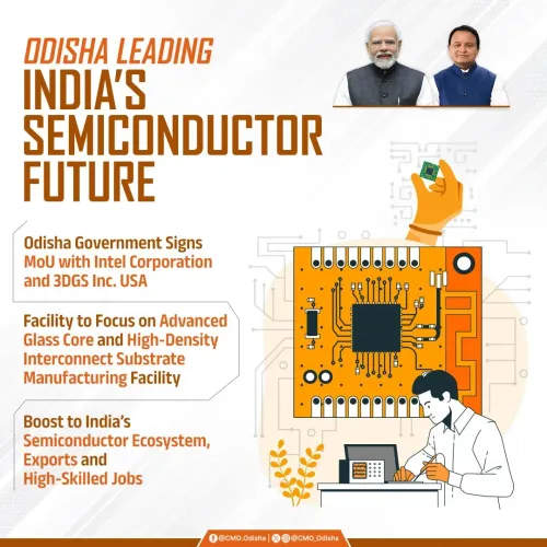
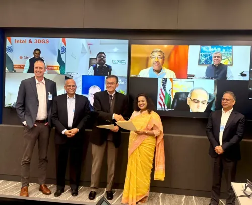
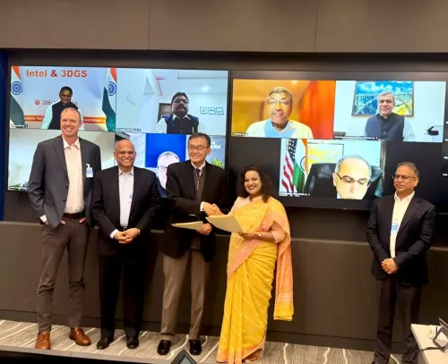
The Odisha government signed an MoU with Intel and 3D Glass Solutions (3DGS) on 29 May for India's first Advanced Packaging Substrate Manufacturing Facility .
The project is expected to attract $3.3 billion in foreign direct investment.
The facility will be located in Bhubaneswar, Khordha district , and will use glass-based substrate and high-density interconnect packaging technologies.
Nearly 1,800 direct high-skilled jobs are expected, along with significant indirect employment.
Intel will provide technology licensing, process expertise, and workforce capability-building support.
The project supports Odisha's targets of a $500 billion economy by 2036 and $1.5 trillion by 2047 .
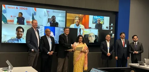
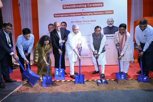
The Odisha government on Friday, 29 May signed a Memorandum of Understanding with Intel and 3D Glass Solutions (3DGS) of the United States for the establishment of an Advanced Packaging Substrate Manufacturing Facility in Bhubaneswar — described by officials as a first-of-its-kind project in India. The deal is expected to bring in foreign direct investment of nearly $3.3 billion, making it one of the largest semiconductor commitments to any Indian state.
What the Facility Will Do
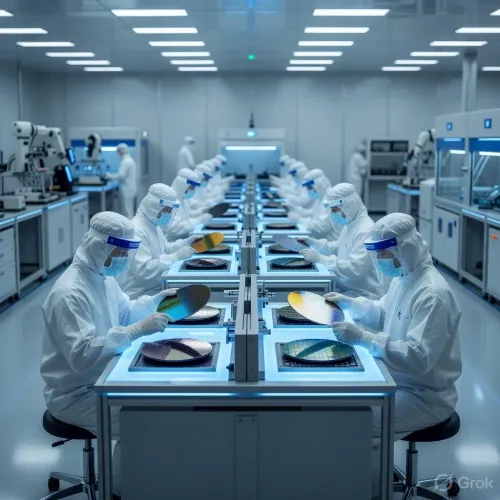
The proposed facility, to be located in Bhubaneswar in Khordha district, will deploy advanced glass-based substrate technologies and high-density interconnect packaging — components considered critical for artificial intelligence, high-performance computing, telecommunications, and next-generation electronics. The plant will house world-class cleanrooms, fabrication units, testing infrastructure, and dedicated research and development (R&D) facilities.
Intel will serve as the technology partner, contributing process expertise, technology licensing, quality systems, and workforce capability-building support. The project will be implemented in phases, with upstream activities spanning advanced materials, specialty chemicals, and capital equipment manufacturing, and downstream activities covering electronics manufacturing and export-oriented industries.
Jobs and Economic Impact
The initiative is expected to generate nearly 1,800 direct high-skilled jobs, along with a significant number of indirect employment opportunities, according to the official statement. Officials noted that the project aligns with Odisha's 'Vision 2036' roadmap, which identifies high-quality, knowledge-based employment as a key pillar of the state's growth strategy.
On the fiscal side, the facility is projected to boost GST collections, expand state revenues through manufacturing and ancillary industries, and strengthen Odisha's long-term export earnings. The government said the project directly contributes to the state's target of becoming a $500 billion economy by 2036 and a $1.5 trillion economy by 2047.
Strategic Significance for India's Semiconductor Push
Advanced packaging is widely regarded as one of the most strategic and fast-evolving segments of the global semiconductor value chain. India has been accelerating efforts to build domestic semiconductor capacity under the Centre's India Semiconductor Mission, and Odisha's MoU with Intel and 3DGS adds a specialised glass-substrate dimension that has so far been absent from the country's manufacturing landscape.
This comes amid intensifying global competition for semiconductor supply chain diversification, with countries across Southeast Asia and South Asia positioning themselves as alternatives to Taiwan and China. Notably, advanced packaging — rather than chip fabrication — has emerged as the entry point of choice for newer manufacturing destinations, given its lower capital threshold relative to front-end fabs.
Ecosystem and Talent Development
Beyond the facility itself, the project is intended to catalyse a broader semiconductor ecosystem in Odisha, attracting global players through cluster-based industrialisation. The initiative is also expected to strengthen academia-industry partnerships and accelerate skill development, creating what officials described as a 'future-ready talent pipeline' aligned with global semiconductor industry demands.
With this agreement, Odisha positions itself as a serious contender for semiconductor and advanced electronics manufacturing leadership in India, integrating the state into global supply chains and reinforcing its strategic importance in the wider technology economy. The next milestone will be the commencement of phased implementation and the finalisation of land and infrastructure arrangements in Khordha district.
Point of View
And India has had no presence in it until now. The Intel partnership lends credibility, but technology licensing agreements are not the same as technology transfer; the depth of Intel's actual commitment will determine whether this becomes a genuine capability or a branding exercise. The 1,800 direct jobs figure also warrants scrutiny against the $3.3 billion investment scale — that ratio suggests a capital-intensive, automation-heavy operation, not a mass-employment one. The real multiplier will come from the downstream ecosystem, and whether Odisha can attract the specialty chemicals and materials suppliers needed to make the cluster self-sustaining.
NationPress
13 Oct 2026
Frequently Asked Questions
What is the Odisha semiconductor MoU with Intel and 3DGS?
The Odisha government signed an MoU with Intel and 3D Glass Solutions (3DGS) of the US on 29 May for the establishment of an Advanced Packaging Substrate Manufacturing Facility in Bhubaneswar — described as the first of its kind in India. The project is expected to bring in nearly $3.3 billion in foreign direct investment and will use glass-based substrate technologies critical for AI, high-performance computing, and next-generation electronics.
What role will Intel play in the Odisha semiconductor facility?
Intel will serve as the technology partner for the project, providing process expertise, technology licensing, quality systems, and workforce capability-building support. Intel will not be the primary investor; 3D Glass Solutions (3DGS) is the principal project partner alongside the Odisha government.
How many jobs will the Odisha semiconductor project create?
The project is expected to generate nearly 1,800 direct high-skilled jobs, along with a significant number of indirect employment opportunities. Officials have linked the initiative to Odisha's 'Vision 2036' roadmap, which prioritises knowledge-based employment generation.
Where will the semiconductor facility be located in Odisha?
The facility will be established in Bhubaneswar, in Khordha district of Odisha. It will house world-class cleanrooms, fabrication units, testing infrastructure, and R&D facilities.
Why is advanced packaging significant for India's semiconductor ambitions?
Advanced packaging is one of the fastest-evolving and most strategically important segments of the global semiconductor value chain, enabling miniaturisation and performance gains for AI and high-performance computing chips. India has so far lacked a domestic advanced packaging capability, making Odisha's glass-substrate facility a first for the country and a potential entry point into global semiconductor supply chains.