Odisha signs MoU with Intel, 3DGS for semiconductor facility
Synopsis
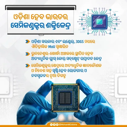
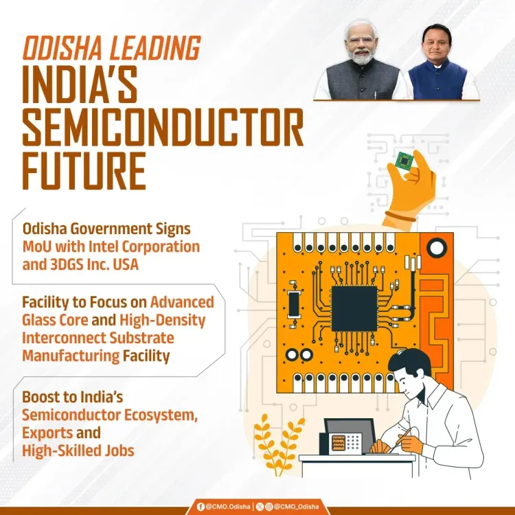
The Government of Odisha signed an MoU with Intel Corporation and 3DGS Inc. on 30 May 2026 to establish an Advanced Packaging Glass Core Substrate Manufacturing Facility, marking a major step in the state's push to become a semiconductor and advanced manufacturing hub under India's national chip mission.
Key Takeaways
The Government of Odisha signed an MoU with Intel Corporation and 3DGS Inc. on 30 May 2026 for an advanced semiconductor packaging facility.
The facility will focus on Glass Core Substrate manufacturing, a critical component in next-generation chip packaging.
The deal aligns with India's India Semiconductor Mission , launched in 2021 with a Rs 76,000 crore outlay to build domestic semiconductor capabilities.
Odisha positions its established steel, mining, and heavy industry base as a logistical advantage for attracting advanced manufacturing investment.
The PMO India was tagged in the official announcement, indicating central government alignment with the initiative.
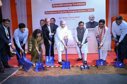
Investment size, groundbreaking timeline, and state incentive packages are yet to be formally announced.
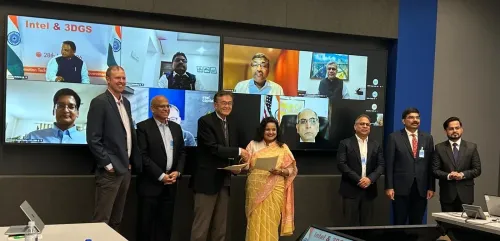
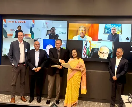
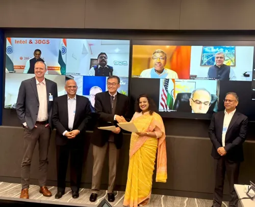
The Chief Minister's Office of Odisha announced on Saturday, 30 May 2026 that the Government of Odisha has signed a landmark Memorandum of Understanding with Intel Corporation and 3DGS Inc. for the establishment of an Advanced Packaging Glass Core Substrate Manufacturing Facility in the state, marking a significant step in Odisha's industrial transformation toward next-generation technologies.
Context
The MoU was formalised between the Government of Odisha, Intel Corporation — one of the world's largest semiconductor companies — and 3DGS Inc., a firm focused on advanced packaging technologies. The agreement envisages setting up a facility dedicated to Glass Core Substrate manufacturing, a critical component in advanced semiconductor packaging that enables higher performance and miniaturisation in chips. The Chief Minister's Office tagged PMO India in the announcement, signalling alignment with the national semiconductor push.
Policy Backdrop
The MoU sits squarely within India's broader semiconductor ambitions. The Government of India launched the India Semiconductor Mission in 2021 with an outlay of Rs 76,000 crore to build domestic chip fabrication, assembly, and test capabilities and reduce the country's heavy dependence on imports. The mission has catalysed a wave of state-level agreements as coastal and industrial states compete to attract semiconductor investment by highlighting infrastructure, port access, and power availability.
Odisha brings a long-established industrial base — anchored in steel, mining, and heavy manufacturing — to this new push. State officials have positioned this foundation as a logistical and workforce advantage for capital-intensive advanced manufacturing projects. The Glass Core Substrate facility would represent a qualitative leap, moving the state up the value chain from raw material processing toward precision electronics production.
Stakeholders and Impact
For Intel Corporation, the Odisha agreement is part of its wider strategy to diversify semiconductor supply chains beyond traditional geographies. Advanced packaging — rather than primary chip fabrication — is a segment where India has been specifically targeted under central incentive schemes, making Odisha a viable location for such investment. 3DGS Inc. brings specialised expertise in the Glass Core Substrate segment, which is increasingly seen as a successor technology to conventional organic substrates in high-end chip packaging.
The facility, once operational, is expected to generate employment opportunities for Odisha's industrial workforce and create a local supplier ecosystem. Semiconductor packaging plants typically require a combination of skilled engineers, precision technicians, and supply-chain support services, offering a broader employment multiplier than primary extraction industries.
What's Next
Attention will now turn to the groundbreaking timeline, the total investment commitment, and any state-level fiscal incentives or skill-development programmes that Odisha may announce to support the facility. The involvement of PMO India in the announcement suggests possible dovetailing with central incentives under the India Semiconductor Mission. How quickly the project moves from MoU to ground-level construction will be a key indicator of the state's ability to execute on its semiconductor ambitions and compete with established electronics manufacturing hubs in Gujarat and Tamil Nadu.
Point of View
Which would accelerate timelines and de-risk the investment for both partners. Whether the MoU converts into ground-level construction at pace will be the real test of Odisha's semiconductor ambitions.
NationPress
15 Oct 2026
Frequently Asked Questions
What is the Odisha MoU with Intel about?
The Government of Odisha signed an MoU with Intel Corporation and 3DGS Inc. on 30 May 2026 to establish an Advanced Packaging Glass Core Substrate Manufacturing Facility in Odisha, aimed at positioning the state as a semiconductor and advanced manufacturing hub.
What is Glass Core Substrate manufacturing?
Glass Core Substrate is a precision material used in advanced semiconductor packaging, enabling higher chip performance and miniaturisation. It is considered a successor to conventional organic substrates in high-end electronics.
How does this relate to India's semiconductor mission?
India launched the India Semiconductor Mission in 2021 with a Rs 76,000 crore outlay to build domestic chip assembly and packaging capabilities. The Odisha MoU aligns with this national strategy to reduce import dependence and attract global semiconductor firms.
What role does Intel play in India's semiconductor plans?
Intel Corporation is one of the world's largest semiconductor companies and has been engaging with India's semiconductor push by exploring advanced packaging investments, which are specifically incentivised under central government schemes.
What will the Odisha semiconductor facility mean for jobs?
Advanced packaging facilities typically require skilled engineers, precision technicians, and supply-chain support, creating an employment multiplier effect. Specific job creation numbers for the Odisha facility have not yet been announced.