Odisha signs semiconductor substrate MoU with Intel and 3DGS
Synopsis
Odisha has quietly become India's most consequential semiconductor state — and the Intel-3DGS substrate MoU cements that. With the country's first 3D chip packaging unit already under construction in Bhubaneswar and now a substrate technology pact in place, Odisha is building the full packaging stack that India's chip ambitions depend on.
Key Takeaways
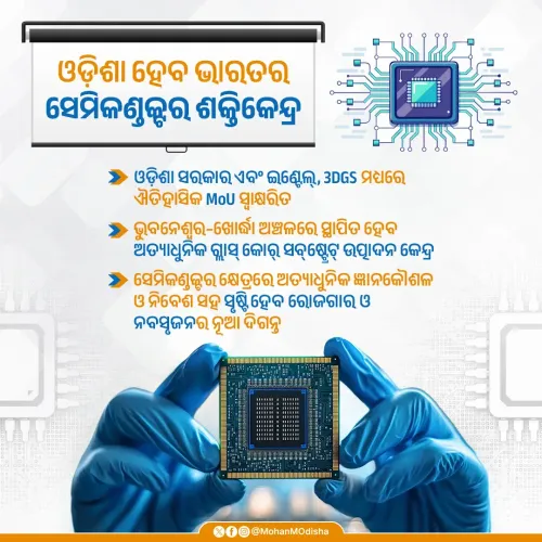
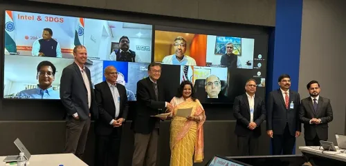
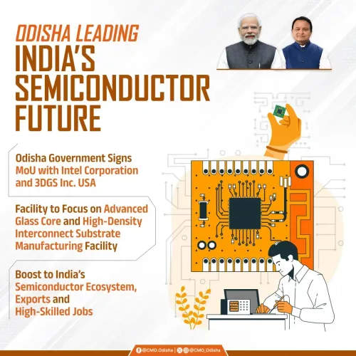
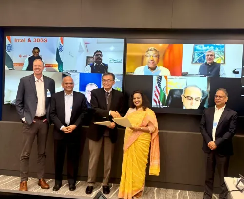
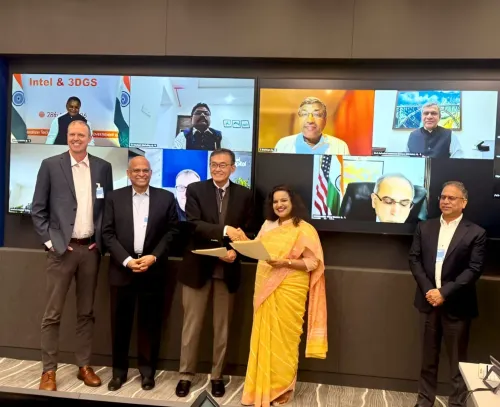
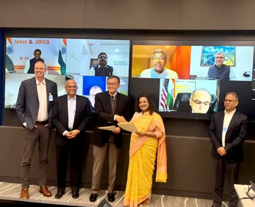
The Odisha government signed an MoU with Intel and 3D Glass Solutions (3DGS) on 29 May to bring semiconductor substrate manufacturing technology to India.
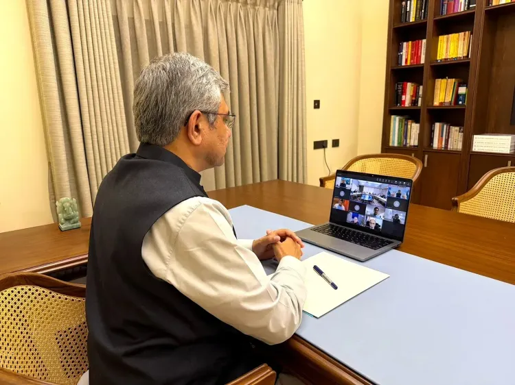
The pact was confirmed by Union Minister Ashwini Vaishnaw via a post on social media platform X.
A related 3DGS project worth nearly ₹2,000 crore at Info Valley, Bhubaneswar targets 70,000 glass panels , 50 million assembled units , and 13,000 3DHI modules annually.
Odisha is the only state hosting both India's first compound semiconductor fabrication unit and first 3D glass substrate packaging facility, according to Chief Minister Mohan Charan Majhi .
Under the Semicon India Programme , 12 fab or packaging projects and 24 semiconductor design projects have been approved nationally.
The Odisha government has signed a memorandum of understanding (MoU) with Intel and 3D Glass Solutions (3DGS) to introduce substrate manufacturing technology in India, Union Minister for Electronics and Information Technology Ashwini Vaishnaw confirmed on Friday, 29 May. The pact marks a significant step in deepening India's domestic semiconductor supply chain.
What the MoU Covers
The agreement is aimed at establishing semiconductor substrate manufacturing capabilities within India, a critical link in the chip production value chain that the country has so far largely imported. Vaishnaw welcomed the development on social media platform X, stating: 'Congratulations to the Govt. of Odisha, Intel and 3DGS on signing an MoU to bring substrate manufacturing technology to India. This will further advance semiconductor ecosystem in India.'
Odisha's Growing Semiconductor Footprint
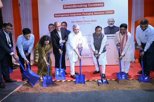
The MoU builds on a series of semiconductor investments Odisha has attracted in recent months. In April, the foundation stone was laid for India's first advanced 3D chip packaging unit at Info Valley in Bhubaneswar, under the Heterogeneous Integration Packaging Solutions project promoted by 3DGS. That project carries an investment of nearly ₹2,000 crore and is expected to produce around 70,000 glass panels annually, along with 50 million assembled units and nearly 13,000 advanced 3D heterogeneous integration (3DHI) modules, according to the government.
Chief Minister Mohan Charan Majhi had noted at the time that Odisha is the only state in the country where both India's first compound semiconductor fabrication unit and first 3D glass substrate packaging facility are being established — a distinction that positions the state as a national anchor for advanced chip manufacturing.
Centre's Semicon India Push
The development comes as the Centre accelerates its efforts to build a self-reliant semiconductor ecosystem under the Semicon India Programme. Earlier this week, the government disclosed that 12 fab or packaging projects and 24 semiconductor design projects have already been approved under the programme. The Centre has also launched an online Investor Support Portal to boost investor confidence and address industry concerns. Vaishnaw had previously stated that under Prime Minister Narendra Modi's leadership, India's semiconductor sector is witnessing rapid growth, with Odisha emerging as a key contributor to the country's chip ambitions.
Why This Matters
Substrate manufacturing is a foundational layer of semiconductor packaging — without domestic capacity, India's chip assembly ambitions remain dependent on foreign supply chains. The Intel and 3DGS partnership signals that global technology majors are willing to transfer advanced manufacturing know-how to India, not just set up assembly lines. This comes amid a global race among nations to onshore semiconductor production following supply chain disruptions that exposed critical dependencies during the pandemic years.
Point of View
24 design projects — are growing, but the real test is whether they add up to an integrated ecosystem or remain isolated islands of capability. Odisha's cluster approach, stacking compound semiconductor fab, 3D packaging, and now substrate manufacturing in one geography, is the right instinct. Execution timelines will be the proof.
NationPress
15 Oct 2026
Frequently Asked Questions
What is the Odisha-Intel-3DGS semiconductor MoU about?
The MoU is an agreement between the Odisha government, Intel, and 3D Glass Solutions (3DGS) to introduce semiconductor substrate manufacturing technology in India. Substrate manufacturing is a key step in chip packaging that India has so far lacked domestic capacity for.
How does this MoU connect to the earlier 3DGS project in Bhubaneswar?
In April 2025, the foundation stone was laid for India's first advanced 3D chip packaging unit at Info Valley in Bhubaneswar, promoted by 3DGS with an investment of nearly ₹2,000 crore. The new MoU builds on that foundation by adding substrate manufacturing technology to Odisha's semiconductor cluster.
What is the Semicon India Programme?
The Semicon India Programme is the Centre's policy framework to develop a domestic semiconductor ecosystem through financial incentives and project approvals. As of this week, 12 fab or packaging projects and 24 semiconductor design projects have been approved under the programme.
Why is Odisha significant in India's semiconductor plans?
Odisha is the only state in India where both the country's first compound semiconductor fabrication unit and first 3D glass substrate packaging facility are being established, according to Chief Minister Mohan Charan Majhi. The new MoU with Intel and 3DGS further strengthens this position.
What will the 3DGS Bhubaneswar project produce?
The 3DGS project at Info Valley in Bhubaneswar is expected to manufacture around 70,000 glass panels annually, along with 50 million assembled units and nearly 13,000 advanced 3D heterogeneous integration (3DHI) modules, according to the government.