Vaishnaw Hails Odisha-Intel-3DGS MoU on Chip Substrates
Synopsis
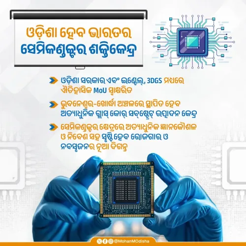
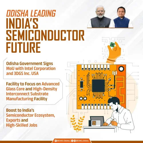
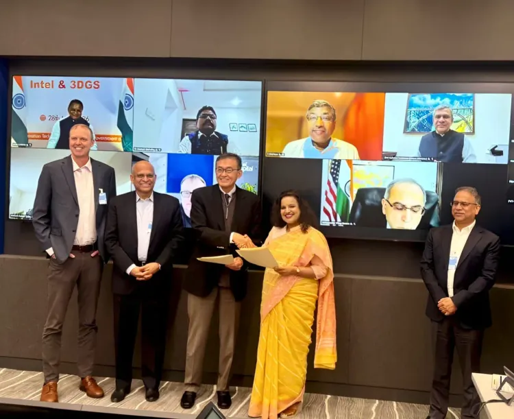
Union Minister Ashwini Vaishnaw welcomed a tripartite MoU between the Government of Odisha, Intel, and 3DGS to bring substrate manufacturing technology to India, advancing the country's semiconductor ecosystem under the India Semiconductor Mission.
Key Takeaways
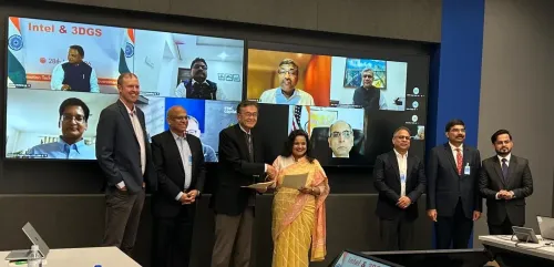
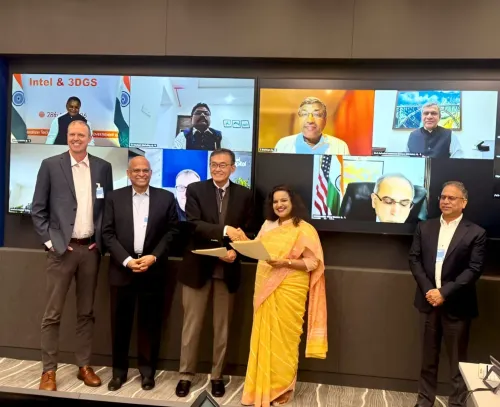
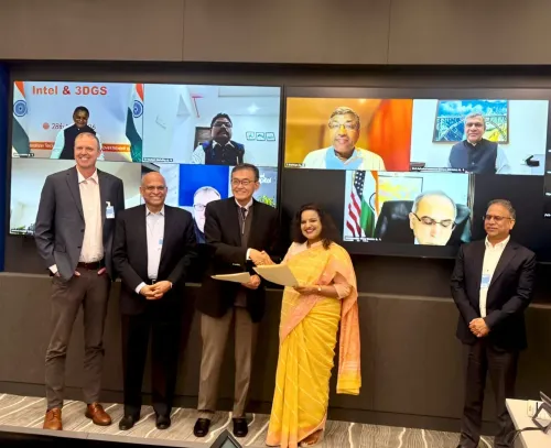
Union Minister Ashwini Vaishnaw congratulated Odisha , Intel , and 3DGS on signing an MoU for substrate manufacturing technology in India on 29 May 2026 .
The agreement covers glass substrate technology for semiconductor packaging and advanced interconnects, an upstream capability critical to next-generation chip production.
The MoU aligns with the India Semiconductor Mission , backed by a Rs 76,000 crore Union Cabinet outlay approved in December 2021 .
Odisha is positioning itself as an emerging semiconductor manufacturing destination through state-level industrial incentives.
Intel already has design and R&D operations in India; this deal extends its footprint into manufacturing-adjacent activity under the ISM framework.
The deal could reduce India's import dependence on semiconductor substrates and serve as a model for future tripartite state-centre-industry agreements.
Union Minister Ashwini Vaishnaw on Friday, 29 May 2026 congratulated the Government of Odisha, Intel, and 3DGS on signing a Memorandum of Understanding to bring substrate manufacturing technology to India, calling it a step that will 'further advance the semiconductor ecosystem in India.'
Context
The tripartite MoU brings together Odisha's state administration, US chipmaker Intel, and 3DGS — a company specialising in glass substrate technology for semiconductor packaging and advanced interconnects. Substrate manufacturing is an upstream capability that enables advanced chip packaging, a segment considered strategically critical as global supply chains diversify away from single-country concentration.
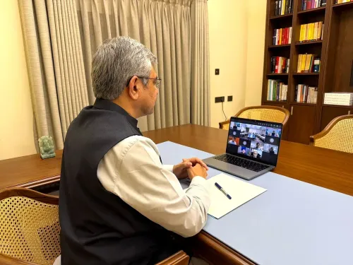
Vaishnaw, who holds the portfolio of Electronics and Information Technology in addition to Railways and Information and Broadcasting, has been a central figure in India's semiconductor push and welcomed the development publicly on X.
Policy Backdrop
The MoU fits squarely within the India Semiconductor Mission (ISM), launched in December 2021 when the Union Cabinet approved an outlay of Rs 76,000 crore to build a domestic chip ecosystem covering design, fabrication, assembly, and substrate technologies. The mission provides financial support and a policy framework intended to make India a viable node in the global semiconductor supply chain.
In 2023-24, the Ministry of Electronics and IT cleared multiple semiconductor and display projects under the Production Linked Incentive scheme, including assembly and packaging units, signalling a phased build-out of the broader value chain. Substrate manufacturing, now anchored partly in Odisha, represents the next layer of that ambition.
Stakeholders and Impact
Odisha has emerged as an unexpected but deliberate destination for electronics and semiconductor-related manufacturing, leveraging state-level industrial policy incentives — including land and power concessions — to complement central fiscal support. The state's inclusion in a deal involving a global name like Intel signals that India's semiconductor strategy is no longer confined to traditional IT hubs such as Bengaluru or Hyderabad.
For Intel, which already operates design and R&D facilities in India, the MoU extends its footprint into manufacturing-adjacent activity under the ISM framework. 3DGS's glass substrate expertise addresses a niche but high-value segment: advanced interconnect substrates that underpin next-generation chip packaging used in AI accelerators and high-performance computing modules. Domestic electronics manufacturers and the broader semiconductor supply chain stand to benefit from reduced import dependence on this input.
What's Next
Analysts and industry stakeholders will watch for further state-level MoUs or central approvals for substrate and packaging projects under the India Semiconductor Mission, as well as any updates in the next semiconductor policy review cycle. The Odisha-Intel-3DGS agreement could serve as a template for similar tripartite arrangements drawing in other states and global chip-supply-chain players.
As India positions itself as an alternative manufacturing hub amid ongoing global chip-supply realignments, the pace at which MoUs translate into operational facilities will be the defining metric of the mission's credibility.
Point of View
Reducing geographic concentration risk while broadening the political dividend of the semiconductor mission. Substrate manufacturing, though unglamorous compared to fab announcements, is a foundational input for advanced packaging; securing it domestically addresses a quiet but significant vulnerability in India's electronics value chain. The broader arc points toward India incrementally climbing the semiconductor value ladder, with each MoU intended to demonstrate investibility to the next wave of global players watching from the sidelines.
NationPress
12 Oct 2026
Frequently Asked Questions
What is the Odisha Intel 3DGS MoU about?
The MoU is an agreement between the Government of Odisha, Intel, and 3DGS to bring substrate manufacturing technology — used in advanced semiconductor packaging — to India, as welcomed by Union Minister Ashwini Vaishnaw on 29 May 2026.
What is 3DGS and what does it do?
3DGS is a company specialising in glass substrate technology for semiconductor packaging and advanced interconnects, a niche segment that supports next-generation chip designs used in AI and high-performance computing.
What is the India Semiconductor Mission?
The India Semiconductor Mission is a central government initiative approved in December 2021 with an outlay of Rs 76,000 crore to develop a domestic semiconductor ecosystem covering chip design, fabrication, assembly, and substrate technologies.
Why is Odisha significant for semiconductor manufacturing?
Odisha has been positioning itself as an emerging electronics and semiconductor manufacturing destination by offering state-level incentives such as land and power concessions to complement central government fiscal support under the India Semiconductor Mission.
What is substrate manufacturing and why does it matter for India?
Substrate manufacturing produces the advanced interconnect layers on which chips are mounted; securing this capability domestically reduces India's import dependence on a critical semiconductor input and supports the broader goal of building a self-reliant chip supply chain.