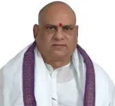
Odisha CM Majhi Signs Intel MoU for Semiconductor Facility
Synopsis
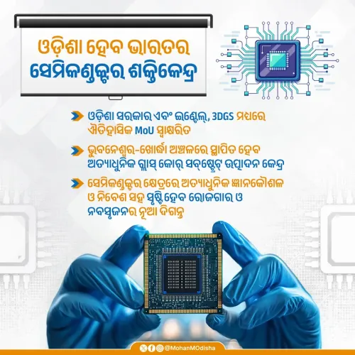
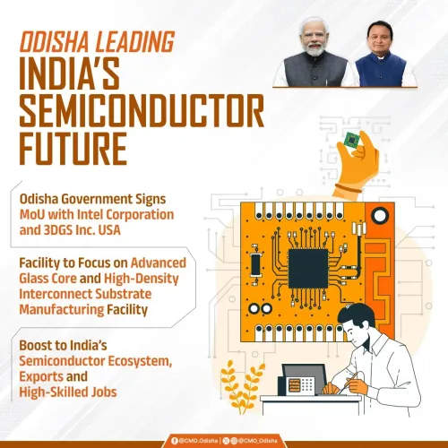
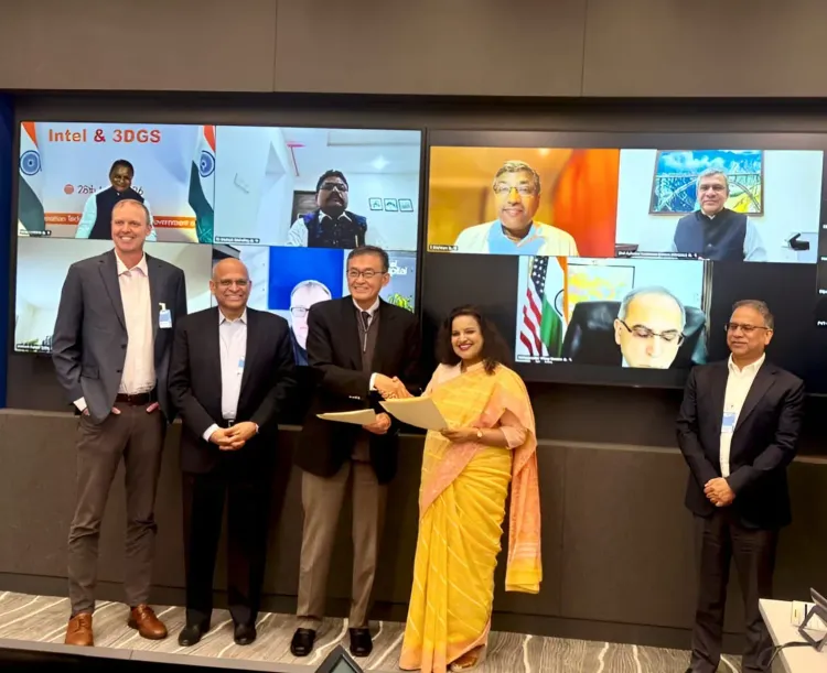
Odisha Chief Minister Mohan Charan Majhi signed an MoU with Intel Corporation and 3DGS Inc. on 29 May 2026 to set up an Advanced Packaging Glass Core Substrate Manufacturing Facility in the Bhubaneswar–Khurda region, advancing India's semiconductor self-reliance mission.
Key Takeaways
Odisha signed an MoU with Intel Corporation and 3DGS Inc. on 29 May 2026 for an Advanced Packaging Glass Core Substrate Manufacturing Facility.
The facility will be located in the Bhubaneswar–Khurda region , a designated electronics and advanced manufacturing corridor.
The investment is aligned with the India Semiconductor Mission , launched in 2021 under MeitY , which offers up to 50 per cent fiscal support for chip manufacturing units.
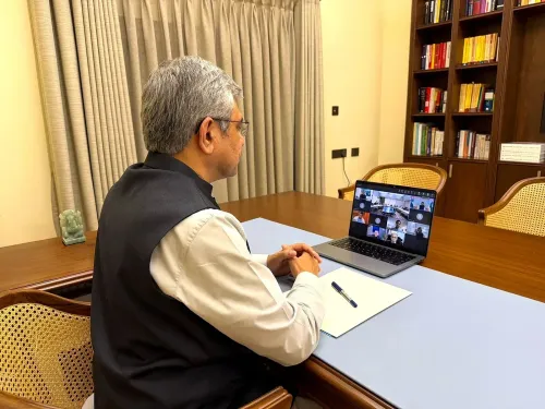
CM Majhi credited the development to the vision of PM Narendra Modi and the support of Union Minister Ashwini Vaishnaw .
The project is expected to create high-skilled employment for Odisha's youth and attract ancillary industries to the region.
Key next steps include a detailed project report to MeitY , land acquisition in Khurda , and vendor tie-ups over the next 12–18 months .
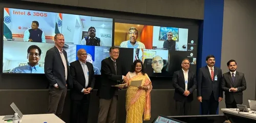
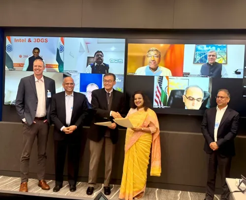
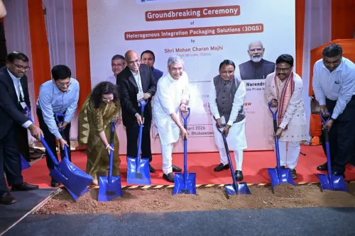
Odisha Chief Minister Mohan Charan Majhi on Friday, 29 May 2026 announced the signing of a Memorandum of Understanding with Intel Corporation and 3DGS Inc. for the establishment of an Advanced Packaging Glass Core Substrate Manufacturing Facility in the Bhubaneswar–Khurda region, marking a significant step in India's semiconductor manufacturing push.
Context
Posting on X, CM Majhi described the development as 'a landmark step towards strengthening India's semiconductor ecosystem and positioning Odisha as a hub for next-generation technology manufacturing.' The MoU brings a globally significant chip-packaging technology — glass core substrate manufacturing — to the state for the first time. Advanced packaging is widely regarded as the next frontier in semiconductor production, enabling faster, smaller and more energy-efficient chips.
The Bhubaneswar–Khurda corridor has been progressively designated for electronics and advanced manufacturing clusters, making it the natural anchor for this investment. The facility is expected to generate high-skilled employment for Odisha's youth and draw ancillary industries into the region.
Policy Backdrop
The announcement is rooted in the India Semiconductor Mission (ISM), launched in 2021 under the Ministry of Electronics and Information Technology (MeitY) to build domestic capacity in chip design, fabrication and packaging with up to 50 per cent fiscal support from the central government. The mission has since catalysed investments across multiple states, with Micron Technology's assembly and test facility in Sanand, Gujarat — announced in 2023 — serving as the first major milestone.
The Production Linked Incentive (PLI) scheme for IT hardware and semiconductors, expanded in 2022–23, has further incentivised global manufacturers to evaluate Indian states as viable manufacturing destinations. Odisha's MoU with Intel and 3DGS Inc. represents the latest and easternmost node in this expanding national semiconductor map.
CM Majhi credited the investment to the vision of Prime Minister Narendra Modi and the support of Union Minister Ashwini Vaishnaw, who oversees semiconductor policy implementation as head of MeitY, framing it as a product of the 'double engine government' model of coordinated central-state action.
Stakeholders and Impact
For Odisha, the facility signals a structural shift away from the state's traditional reliance on mining, steel and aluminium toward high-value knowledge-driven industries. Young engineers and technically skilled workers stand to be the primary beneficiaries of the employment opportunities the plant is expected to generate. Ancillary sectors — precision components, logistics, specialised chemicals — are also likely to develop around the core facility.
For Intel Corporation, which has been deepening its foundry and packaging partnerships globally, a presence in Bhubaneswar aligns with its strategy to diversify manufacturing geography beyond the United States, Europe and East Asia. 3DGS Inc., a specialist in glass core substrate technology, brings the advanced packaging expertise central to the project's technical proposition.
At the national level, the MoU strengthens India's case as a credible alternative in global semiconductor supply chains at a time when governments worldwide are incentivising chip-manufacturing diversification.
What's Next
The immediate milestones will include submission of a detailed project report to MeitY, land acquisition processes in Khurda, and the formalisation of vendor and OSAT (Outsourced Semiconductor Assembly and Test) tie-ups. Industry observers expect these steps to unfold over the next 12 to 18 months. How swiftly the state government clears regulatory and land-related hurdles will determine whether Odisha can convert this MoU into an operational facility ahead of competing regional destinations. If the project reaches production scale, it could position Bhubaneswar as eastern India's first significant node in the global semiconductor value chain.
Point of View
And it fits a deliberate BJP pattern of routing central semiconductor incentives through state governments to generate visible development dividends. By anchoring the facility in Bhubaneswar–Khurda, the state is attempting to replicate the Gujarat semiconductor playbook in eastern India, diversifying the national chip-manufacturing map beyond its current western concentration. The explicit invocation of PM Modi and Ashwini Vaishnaw signals that credit-sharing between the central and state governments is built into the political architecture of this deal. Whether the MoU translates into operational capacity will hinge on execution speed — land clearances, regulatory approvals and supply-chain readiness — factors that have historically separated announcements from outcomes in Indian industrial policy.
NationPress
14 Oct 2026
Frequently Asked Questions
What did Odisha sign with Intel Corporation?
Odisha signed an MoU with Intel Corporation and 3DGS Inc. on 29 May 2026 for the establishment of an Advanced Packaging Glass Core Substrate Manufacturing Facility in the Bhubaneswar–Khurda region.
Where will the Intel semiconductor facility in Odisha be located?
The facility will be located in the Bhubaneswar–Khurda region, which has been designated as an electronics and advanced manufacturing corridor in Odisha.
What is the India Semiconductor Mission?
The India Semiconductor Mission is a central government scheme launched in 2021 under MeitY to build domestic capacity in chip design, fabrication and packaging, offering up to 50 per cent fiscal support to qualifying projects.
What is glass core substrate technology?
Glass core substrate is an advanced semiconductor packaging technology that enables faster, smaller and more energy-efficient chips compared to conventional organic substrates, and is considered a next-generation advancement in chip manufacturing.
How does the Odisha Intel MoU fit into India's semiconductor strategy?
The MoU extends India's semiconductor manufacturing footprint to eastern India, complementing earlier investments in Gujarat and other states under the India Semiconductor Mission and PLI schemes, as India seeks to build a diversified domestic chip supply chain.