IBM unveils world's first sub-1nm chip, packs 100bn transistors

Synopsis
IBM has crossed what many considered an uncrossable line — the sub-1 nanometre barrier. Its 0.7 nm nanostack chip nearly doubles the transistor density of its own 2021 breakthrough, and promises either 50% more speed or 70% less power consumption. With generative AI and cloud infrastructure hungry for exactly this kind of leap, the five-year commercial clock has started.
Key Takeaways
IBM unveiled the world's first sub-1 nanometre (0.7 nm) chip technology on Thursday, 25 June .
The chip packs nearly 100 billion transistors — almost double the density of IBM's 2 nm chip from 2021.
The new nanostack architecture vertically stacks transistors, optimising materials independently for performance and power.
Performance gains projected at up to 50% higher speed or 70% greater energy efficiency versus the 2 nm node.
Research was conducted at IBM's facility in Albany, New York , with partners including ASML , Lam Research , Tokyo Electron , and SCREEN Semiconductor Solutions .
Commercial adoption is expected within the next five years , targeting generative AI , cloud , and next-gen consumer devices.
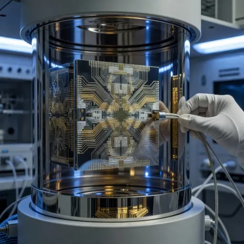
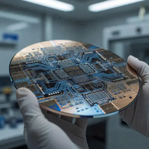
IBM on Thursday unveiled what it describes as the world's first sub-1 nanometre chip technology, a landmark advance for the global semiconductor industry as it pushes past the physical limits of conventional chip scaling. The new process node, built at 0.7 nm — or 7 angstroms — introduces a novel three-dimensional transistor architecture that IBM calls nanostack.
What the Breakthrough Delivers
The 0.7 nm chip packs nearly 100 billion transistors onto a device roughly the size of a fingernail, almost doubling the transistor density of IBM's own 2 nm chip unveiled in 2021. According to the company, the new node is projected to deliver up to 50 per cent higher performance or 70 per cent greater energy efficiency compared to its 2 nm predecessor.
How the Nanostack Architecture Works
IBM's nanostack design vertically stacks and staggers transistors, enabling more components to be packed into a smaller footprint while allowing different materials to be optimised independently for performance and power. IBM researchers also demonstrated that the architecture can significantly improve SRAM scaling, which is critical for building processors capable of handling high-bandwidth AI workloads.
Jay Gambetta, Director of IBM Research and IBM Fellow, described the development as a defining shift: 'IBM's latest chip breakthrough marks a landmark moment in computing, pushing technology beyond the nanometre era to the scale of atoms.'
Where It Was Developed
The research was conducted at IBM's semiconductor research facility in Albany, New York, in collaboration with industry partners including ASML, Lam Research, Tokyo Electron, and SCREEN Semiconductor Solutions. The involvement of these major equipment makers signals that the technology has already cleared early-stage manufacturing feasibility checks.
Applications and Commercial Timeline
IBM says the technology is designed to support demanding workloads including generative AI, cloud infrastructure, and next-generation consumer electronics. The company expects the earliest commercial adoption within the next five years. Notably, this timeline aligns with broader industry projections for when current 2 nm and 3 nm nodes will begin hitting performance ceilings. The 0.7 nm node, if it reaches volume production, would represent the most significant leap in transistor density since the introduction of FinFET architecture over a decade ago.
Point of View
But the distance between a research demonstration in Albany and volume production at a foundry is vast — a gap that has swallowed many headline-grabbing chip milestones before it. The five-year commercial window is notably vague, and IBM no longer operates its own leading-edge fabs at scale, which means the real test will be whether partners like ASML and Lam Research can translate the nanostack architecture into a manufacturable process. The AI industry's insatiable demand for denser, more efficient silicon gives IBM a commercial pull it lacked in previous research cycles — but execution, not the lab result, will determine whether this becomes a foundry inflection point or another impressive paper.
NationPress
25 Jun 2026
Frequently Asked Questions
What is IBM's sub-1 nanometre chip technology?
It is a semiconductor process node built at 0.7 nm (7 angstroms), featuring a novel three-dimensional transistor design IBM calls nanostack. The chip packs nearly 100 billion transistors onto a fingernail-sized device, nearly doubling the density of IBM's own 2 nm chip from 2021.
What is the nanostack architecture?
Nanostack is IBM's three-dimensional transistor design that vertically stacks and staggers transistors, allowing more components per unit area while enabling different materials to be independently optimised for performance and power efficiency. It also improves SRAM scaling for AI-intensive workloads.
When will IBM's 0.7nm chip be commercially available?
IBM expects the earliest commercial adoption of the technology within the next five years. The company has not announced a specific production partner or foundry timeline.
What performance improvements does the 0.7nm chip offer?
According to IBM, the new node can deliver up to 50 per cent higher performance or 70 per cent greater energy efficiency compared to its 2 nm chips, depending on how the design is optimised.
Where was the IBM chip research conducted and who were the partners?
The research was carried out at IBM's semiconductor facility in Albany, New York, in collaboration with ASML, Lam Research, Tokyo Electron, and SCREEN Semiconductor Solutions — all major players in chip manufacturing equipment.