VIHAAN chip: DLI-backed Aheesa scores first-pass silicon success for India
Synopsis
On Independence Day, a Chennai startup achieved something most chip designers dread failing at — first-pass silicon success. Aheesa's VIHAAN SoC, designed for fibre broadband, is now on track for production tape-out by 2027, backed by ₹40 crore in funding and the government's DLI Scheme. It is a small but concrete signal that India's semiconductor design ambitions are moving from policy to silicon.
Key Takeaways
Aheesa Digital Innovations achieved first-pass silicon success for its VIHAAN networking SoC on 15 August 2025 , confirmed by MeitY .
The chip, designed for fibre broadband applications, was taped out on Republic Day and is targeted for production tape-out by 2027 .
Aheesa raised approximately ₹40 crore from the Tamil Nadu Emerging Sector Seed Fund and private investors earlier this year.
DLI Scheme-backed companies have collectively completed more than 30 tape-outs and raised over $100 million in venture capital.
The government's Semicon 2.0 scheme, approved in July , carries a ₹1,27,500 crore outlay to build a full-stack semiconductor ecosystem.
Chip-design tools are now available to 455 organisations , including 350 academic institutions and 105 startups .
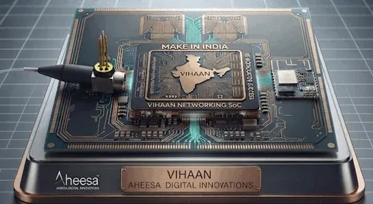
Chennai-based fabless semiconductor startup Aheesa Digital Innovations has achieved first-pass silicon success for its VIHAAN networking system-on-chip (SoC), a milestone that underscores the growing depth of India's indigenous chip design ecosystem. The achievement, announced on 15 August 2025, was confirmed by the Ministry of Electronics and Information Technology (MeitY), which noted the chip is designed for fibre broadband applications and will now advance toward production tape-out, targeted for 2027.
The VIHAAN Chip: Key Milestones
The VIHAAN SoC has a symbolic arc to its development: the chip was taped out on Republic Day and achieved first-pass silicon success on Independence Day this year. First-pass silicon success — where a chip works as intended on its very first physical fabrication run — is a significant engineering achievement, as failures at this stage typically cost startups months and considerable capital.
Aheesa is developing semiconductor solutions for broadband networking and security, sectors that are central to India's ongoing digital infrastructure expansion through optical fibre, 5G, and broadband-led services, according to the ministry.
DLI Scheme Backing and Investor Support
Aheesa's progress has been supported by the government's Design Linked Incentive (DLI) Scheme, which is backing Indian startups developing chips for strategic and commercial applications — including satellite communications, drones, surveillance cameras, defence and aerospace systems, automotive electronics, Internet of Things devices, artificial intelligence, telecom equipment, and smart meters.
Beyond government support, the startup has attracted private capital: it raised approximately ₹40 crore earlier this year from the Tamil Nadu Emerging Sector Seed Fund and other private investors to accelerate product development and scale its semiconductor business.
Broader Ecosystem Gains
The VIHAAN milestone is not an isolated success. Companies supported under the DLI Scheme have cumulatively achieved more than 30 chip design tape-outs across various foundries and raised over $100 million in venture capital funding, according to the ministry statement.
Chip-design tools have been made available to 455 organisations — including 350 academic institutions and 105 startups — under government semiconductor programmes. Separately, 245 chip designs have been taped out by 71 academic institutions under the Chips to Startup programme.
Other recent milestones in the Indian semiconductor space include Vervesemi Microelectronics' motor controller chip, Netrasemi's 12 nm Vision SoC, and OptoML's 12 nm compute-in-memory SoC, reflecting a broadening pipeline of domestic chip innovation.
Semicon 2.0 and the Strategic Context
The government approved the Semicon 2.0 scheme in July with a ₹1,27,500 crore outlay, aimed at building a globally competitive semiconductor ecosystem spanning chip design, manufacturing, advanced packaging, equipment, materials, research and development, and skilled manpower.
Notably, the ministry highlighted that semiconductor chip design can contribute up to 50 per cent of overall value addition across the semiconductor value chain, and accounts for approximately 15–35 per cent of the bill of materials cost of electronic products — making indigenous design capability a high-leverage strategic priority.
With production tape-out targeted for 2027, the VIHAAN chip's commercial trajectory will be a closely watched indicator of whether India's semiconductor design push can translate from laboratory milestones to market-ready products at scale.
Point of View
Not just a press release milestone. The harder question is whether India's ecosystem can sustain this momentum through to commercial volumes: tape-out targets and production timelines are routinely delayed in semiconductor development, and the gap between a working chip and a chip in a product is where most startups stall. The Semicon 2.0 outlay is large, but capital alone does not build the packaging, testing, and supply-chain depth that turns design wins into industry. The 2027 production tape-out date for VIHAAN will be the real test of whether DLI support translates into durable commercial capability.
NationPress
30 Sept 2026
Frequently Asked Questions
What is the VIHAAN chip developed by Aheesa Digital Innovations?
VIHAAN is a networking system-on-chip (SoC) designed by Chennai-based fabless startup Aheesa Digital Innovations for fibre broadband applications. It achieved first-pass silicon success on 15 August 2025 and is targeted for production tape-out by 2027.
What is the Design Linked Incentive (DLI) Scheme?
The DLI Scheme is a Government of India programme that supports domestic semiconductor startups in developing chips for strategic and commercial applications, including telecom, defence, automotive, IoT, and AI. Companies backed by the scheme have collectively completed over 30 tape-outs and raised more than $100 million in venture capital.
How much funding has Aheesa raised?
Aheesa raised approximately ₹40 crore earlier in 2025 from the Tamil Nadu Emerging Sector Seed Fund and other private investors to accelerate product development and scale its semiconductor operations.
What is the Semicon 2.0 scheme approved by the government?
Semicon 2.0 is a government scheme approved in July 2025 with a ₹1,27,500 crore outlay. It aims to build a globally competitive semiconductor ecosystem covering chip design, manufacturing, advanced packaging, equipment, materials, R&D, and skilled manpower.
What other Indian semiconductor milestones have been reported recently?
Recent achievements include Vervesemi Microelectronics' motor controller chip, Netrasemi's 12 nm Vision SoC, and OptoML's 12 nm compute-in-memory SoC. Additionally, 245 chip designs have been taped out by 71 academic institutions under the Chips to Startup programme.