Cabinet Approves Semicon 2.0 With ₹1,27,500 Cr Outlay
Synopsis
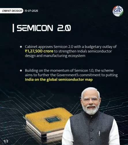
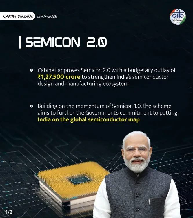
The Union Cabinet chaired by PM Narendra Modi has approved Semicon 2.0, allocating ₹1,27,500 crore to develop India's semiconductor design and manufacturing ecosystem — a near-68% jump over the original 2021 Semicon India programme of ₹76,000 crore.
Key Takeaways
The Union Cabinet, chaired by PM Narendra Modi , approved Semicon 2.0 on 15 July 2026 .
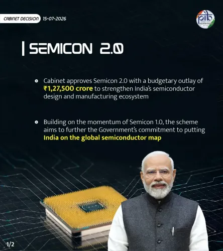
The programme carries a total budget outlay of ₹1,27,500 crore , targeting semiconductor design and manufacturing.
This represents a near- 68 per cent increase over the original Semicon India programme approved in December 2021 with an outlay of ₹76,000 crore .
The India Semiconductor Mission is the nodal body overseeing implementation, including design-linked incentives and fab project approvals.
The move aims to reduce India's reliance on chip imports from Taiwan , South Korea , and China .
Minister Sarbananda Sonowal announced the Cabinet decision via his official X account on 15 July 2026 .
Union Ports and Shipping Minister Sarbananda Sonowal announced on Wednesday, 15 July 2026 that the Union Cabinet, chaired by Prime Minister Narendra Modi, has approved Semicon 2.0 — a major expansion of India's semiconductor design and manufacturing ecosystem — with a total budget outlay of ₹1,27,500 crore.
Context
The Cabinet decision marks a significant scaling-up of India's ambitions in the global semiconductor race. Sonowal shared the announcement on X (formerly Twitter), noting the approval under #CabinetDecisions, confirming that the programme targets both semiconductor design and manufacturing capacity within India.
The move comes as India seeks to establish itself as a credible alternative to established chip-manufacturing hubs in Taiwan, South Korea, and China, reducing its dependence on imports that were severely disrupted during the COVID-19 pandemic.
Policy Backdrop
India's semiconductor push has its roots in the original Semicon India programme, approved by the Union Cabinet in December 2021 with an initial outlay of ₹76,000 crore. That programme was anchored under the India Semiconductor Mission, a dedicated body set up to attract fabrication, assembly, testing, marking, and packaging (ATMP) investments.
Semicon 2.0 represents a substantial expansion — the new outlay of ₹1,27,500 crore is nearly 68 per cent higher than the original programme — reflecting both the scale of global competition and the urgency India places on chip self-reliance under the broader Atmanirbhar Bharat framework championed by Prime Minister Modi.
The programme is expected to deepen design-linked incentives alongside manufacturing subsidies, addressing a gap in India's semiconductor value chain where design talent has historically outpaced domestic fabrication capacity.
Stakeholders and Impact
The primary beneficiaries of Semicon 2.0 are domestic and international semiconductor firms, electronics manufacturers, and the broader component supply chain that feeds into consumer electronics, automotive, defence, and telecom sectors.
India's engineering talent base — already a significant presence in global chip design — stands to gain from enhanced design-linked incentive structures, potentially attracting global semiconductor companies to establish or expand design centres in the country.
For electronics manufacturers operating in India, greater domestic chip availability would reduce procurement lead times and currency-exposure risks currently tied to dollar-denominated imports from East Asia.
What's Next
Attention now turns to the India Semiconductor Mission, which is expected to roll out detailed guidelines for design-linked incentives and invite fresh applications for fabrication projects under the expanded programme.
Analysts will watch for announcements of new fab project approvals, potential partnerships with global chipmakers, and state-level complementary incentive packages — particularly from Gujarat and Telangana, which have previously positioned themselves as semiconductor investment destinations.
With ₹1,27,500 crore committed, Semicon 2.0 sets the stage for India's most consequential industrial policy bet in the technology sector, with implications for employment, export competitiveness, and strategic autonomy in critical technology supply chains.
Point of View
27,500 crore is the Modi government's clearest signal yet that semiconductor self-reliance has moved from aspiration to industrial priority. The near-doubling of financial commitment over the 2021 baseline reflects lessons learned from the first programme's slow uptake and global competition from the US CHIPS Act and European Chips Act. By bundling design incentives with manufacturing support, the government is attempting to close a structural gap that has long limited India's chip ambitions to talent export rather than domestic value creation. The scale of the outlay will test the India Semiconductor Mission's administrative bandwidth and the market's appetite for large-scale fab investments on Indian soil.
NationPress
15 Jul 2026
Frequently Asked Questions
What is Semicon 2.0 approved by the Cabinet?
Semicon 2.0 is a government programme approved by the Union Cabinet on 15 July 2026 to develop India's semiconductor design and manufacturing ecosystem, with a total budget outlay of ₹1,27,500 crore.
How much money has India allocated for semiconductor manufacturing under Semicon 2.0?
The Cabinet has approved a total outlay of ₹1,27,500 crore for Semicon 2.0, significantly higher than the ₹76,000 crore committed under the original Semicon India programme in December 2021.
What is the India Semiconductor Mission?
The India Semiconductor Mission is the nodal government body set up to attract and facilitate investments in semiconductor fabrication, assembly, testing, and design in India, and will oversee implementation of Semicon 2.0.
Why is India investing in semiconductor manufacturing?
India is investing in domestic chip production to reduce dependence on imports from Taiwan, South Korea, and China, and to build strategic resilience in critical technology supply chains after disruptions exposed during the COVID-19 pandemic.
Who announced the Semicon 2.0 Cabinet decision?
Union Minister Sarbananda Sonowal announced the Cabinet approval of Semicon 2.0 on his official X account on 15 July 2026, citing the decision taken under the chairmanship of PM Narendra Modi.