

India targets indigenous GPU in 2 years under Semiconductor Mission 2.0
Synopsis
India is targeting its own GPU within two years — a bold leap from server assembly to chip design. With 12 semiconductor projects approved, five in production, ASML and Intel tied to Tata, and C-DAC's Rudra servers already running AI workloads, Semicon 2.0 is shaping up as the most consequential industrial bet in India's tech history.
Key Takeaways
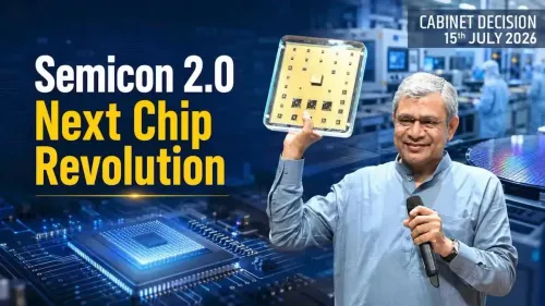
India has set a 2-year target to develop an indigenous GPU under the upcoming India Semiconductor Mission 2.0 .
Krishnan confirmed the milestone, calling it a complex but achievable undertaking.
12 semiconductor manufacturing projects have been approved; 5 are already in commercial production.
ASML is partnering with Tata Electronics for India's first commercial fab in Dholera, Gujarat , targeting 50,000 wafers per month .
Intel has entered a strategic partnership with the Tata Group for semiconductor manufacturing and packaging.
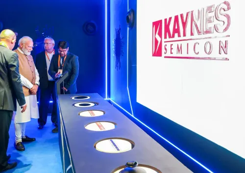
C-DAC's Rudra server platforms and domestic production by VVDN Technologies , Kaynes Technology , and Avalon Technologies signal early AI hardware capability.
India has set a target of developing its own graphics processing unit (GPU) within the next two years as part of a broader drive to deepen domestic semiconductor capabilities and reduce dependence on foreign chipmakers, according to Electronics and Information Technology Secretary S. Krishnan. The initiative is planned under the upcoming India Semiconductor Mission 2.0 (ISM 2.0).
The GPU Development Plan
Speaking in an interview, Krishnan acknowledged that building a homegrown GPU is a complex undertaking but confirmed the government has set a firm milestone of roughly 24 months. The move signals a qualitative leap for India's semiconductor ambitions — from assembly and packaging toward advanced chip design. A domestically developed GPU would have direct applications in artificial intelligence (AI) workloads, data centres, and defence computing, areas where India currently relies almost entirely on imported silicon.
Early Progress in AI Hardware
India has already built a nascent foundation in AI-related hardware. Companies including VVDN Technologies, Kaynes Technology, and Avalon Technologies are producing servers domestically. The Centre for Development of Advanced Computing (C-DAC) has developed its Rudra server platforms, purpose-built for AI workloads, underscoring that some indigenous capability already exists at the system level.
Semicon 2.0: Beyond Manufacturing
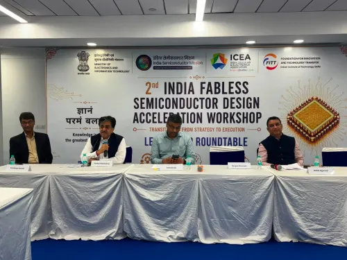
Amitesh Kumar Sinha, Additional Secretary at the Ministry of Electronics and Information Technology (MeitY) and CEO of the India Semiconductor Mission (ISM), outlined the broader contours of the strategy on 5 November 2026 at the ISIG Executive Summit India 2026. He said India's semiconductor push has moved from policy design to active ecosystem-building, with 12 manufacturing projects approved, of which five have already begun commercial production.
"Semicon 2.0 is about building the broader ecosystem, including design companies, materials, chemicals, gases and equipment, alongside manufacturing, R&D and talent," Sinha said.
Global Partners Anchoring India's Fab Ambitions
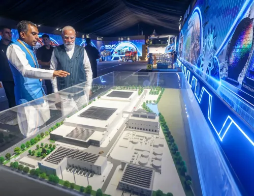
Major global players are aligning with India's semiconductor roadmap. Dutch equipment giant ASML is partnering with Tata Electronics to support India's first commercial semiconductor fabrication facility in Dholera, Gujarat. The fab is designed to use 300mm wafers and is expected to eventually reach a production capacity of 50,000 wafers per month. Intel has also entered a strategic partnership with the Tata Group covering semiconductor manufacturing and packaging.
What This Means for India's Tech Ambitions
This comes amid intensifying global competition for semiconductor self-sufficiency, with the United States, China, and the European Union each running aggressive chip subsidy programmes. India's two-year GPU target, if achieved, would mark a significant inflection — moving the country from a consumer of chip technology to a contributor to its design. The next key milestones to watch are the formal launch of ISM 2.0 and the commissioning timeline of the Dholera fab.
Point of View
ASML, and Intel-Tata give the country genuine manufacturing footing for the first time. The GPU ambition, however, risks becoming a headline target that overpromises and underdelivers unless MeitY pairs it with a credible design-house pipeline and competitive talent retention — two areas where India's semiconductor policy has historically been thin.
NationPress
9 Nov 2026
Frequently Asked Questions
What is India's plan to develop an indigenous GPU?
India aims to design and develop its own graphics processing unit (GPU) within two years as part of the India Semiconductor Mission 2.0, according to IT Secretary S. Krishnan. The GPU is intended to support AI workloads and reduce India's dependence on foreign chipmakers.
What is India Semiconductor Mission 2.0?
India Semiconductor Mission 2.0 (Semicon 2.0) is the next phase of India's national chip strategy, focused on building a full ecosystem beyond manufacturing — covering design companies, materials, chemicals, gases, equipment, R&D, and talent. It follows an earlier phase under which 12 manufacturing projects were approved.
How many semiconductor projects are operational in India?
Of the 12 semiconductor manufacturing projects approved under India's semiconductor mission, five have already commenced commercial production, according to ISM CEO Amitesh Kumar Sinha, speaking at the ISIG Executive Summit India 2026 on 5 November 2026.
What is the Dholera semiconductor fab and who is involved?
The Dholera fab, located in Gujarat, is set to be India's first commercial semiconductor fabrication facility. It is being developed by Tata Electronics in partnership with Dutch equipment maker ASML, using 300mm wafers with a targeted capacity of 50,000 wafers per month.
How does C-DAC's Rudra server fit into India's semiconductor strategy?
C-DAC's Rudra is a domestically developed server platform optimised for AI workloads, representing India's existing capability at the system level. It complements broader efforts by companies like VVDN Technologies, Kaynes Technology, and Avalon Technologies, which are already manufacturing AI servers in India.